Analog System Design Project
The focus on this fourth design project is to
develop a design of an analog system.
Analog System Design Project Description
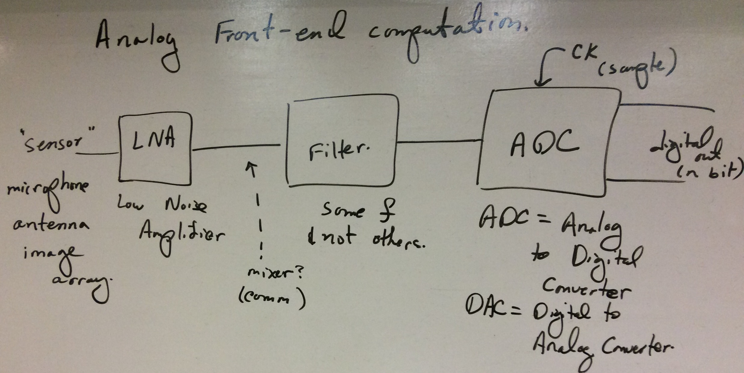
In this project, we are going to be building a typical analog system chain.
In particular, we will be looking at a typical chain from an input analog sensor
until it gets to a digital signal,
by far, the most common of analog input chains.
Each team will be building block(s) of the resulting system.
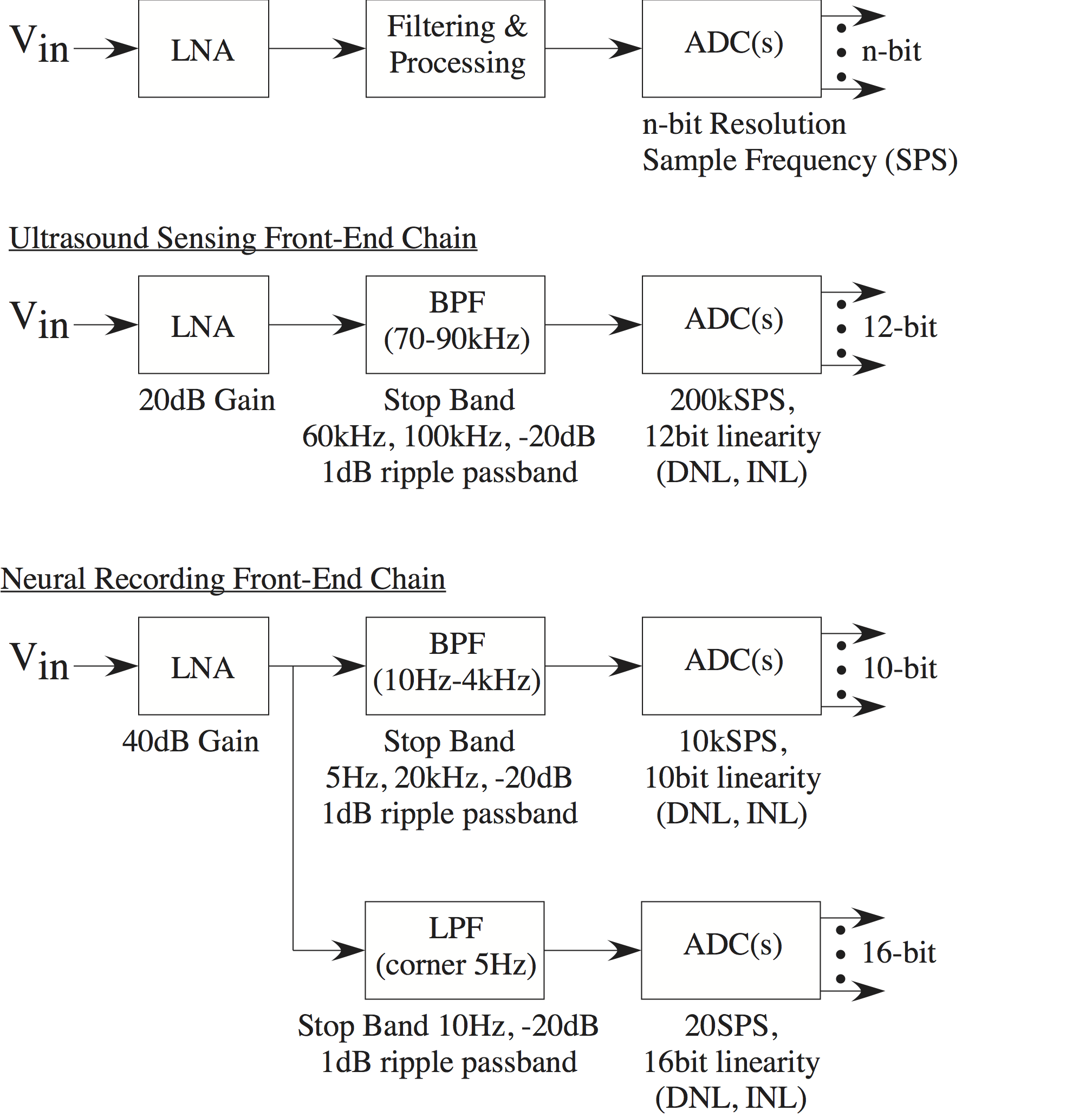
Figure 1:
Block diagram of the basic framework for an analog signal processing chain for an input sensor,
and representative block diagrams
for an ultrasound sensing application,
and for a neural probe sensing application.
In both examples, we list some typical specs required in these cases.
For this project, we will be focusing on the neural measurement chain,
particularly the higher frequency half of that chain.
Figure 1 shows a typical analog system block for sensor inputs.
Such a system would be typical if we were using a temperature sensor,
a microphone sensor,
ultrasound sensor,
sensing data from a hard drive,
or even sensing wireless signals.
For all designs, optimizing power consumed as well as area are critical for both designs.
The power supply for the IC will be 2.5V, just like our FPAA IC.
As this design is a physical design, you should be aware of design mismatch on your IC,
where appropriate.
Anotherwords, one could (and we might) put this block on a different FPAA IC than you
designed your block.
You should minimize the number of CABs and CAB components required for your design (area),
meet the resulting metrics, and minimize the required power consumed.
You should discuss the effect of temperature on your design, if it is present at all.
You effectively do not have any explicit
inductors or resistors.
Having used these FPAA devices in the past, you know you have stable voltage references.
We have previous described approaches for stable current references.
Between the two cases, we will have six different blocks, resulting in 6 different design teams from the class that I will be assigning.
Application1: Front-end System design for Neural Recording
Figure 1
the block diagram to build an analog system design for sensing neural recording.
Typically we would want many of these probes, but we will concentrate on the design of a single input for this problem.
In these applications, power is really critical, since often the power is wirelessly inductively coupled to the circuit,
and as a result, we want to use as little power as required.
LNA stage:
We are looking at typical input signals that are roughly 1mV and we want an SNR of 60dB.
We would want an LNA with 40dB of gain to bring the maximum signal to 100mV, which can be handled and not creating that much distortion.
The dc signal, at the frequencies associated with changes over minutes and hours, could change significantly (1-100mV input change),
and must be eliminated from the incoming signal at the LNA stage.
We expect the output signal into the next stage is a peak of 100mV,
with the output SNR of this stage being 60dB.
We don't expect nonlinearities to be an issue for this stage.
Filter Stage:
We will want two different signal paths coming from the LNA signal. One path is for identifying the action potentials, so looking at frequencies above 10Hz.
The second path is for identifying low frequency waves going through the neural tissue, so we are looking at frequencies of 5Hz and below. We see similar type designs for EEG approaches.
The specifications are shown in 1.
We expect both of the filters to output a signal
that is maximum at 1.5V peak to peak in the power supply.
Remember the peak input voltage would be expected to be 100mV.
The signal must be away from the power supply rails by 300mV. The input from the LNA won't necessarily have a well defined DC point, so your filter must handle these issues.
This issue won't be a problem for your bandpass filter.
The signal being away from the power supply rails by 300mV
means that you're input common mode range should be from 300mV to 2.2V,
because the DC isn't defined and can vary.
You don't need rail to rail input stage for your OTA,
but a reasonably wide input range is important.
In terms of gain, you should realize your starting input signal could be as big at 100mV (pk-pk).
Your output signal will be max of 1.5V (pk-pk).
Therefore your gain needs to be 15 between input and output of your filter.
Your bandpass filters might have intrinsic gain depending on the topology you pick (i.e. Look at the paper put up today).
Distortion for a 100mV input sinusoidal signal in the band of interest should be at least -40dB below the primary harmonic for a two-tone test.
The SNR needs to be 60dB SNR from the output filter.
Because of distortion, the amplifier will multiply these signals internally, and you will see their products in the spectrum.
The distortion measurement in this case is whats called a two-tone test which is used to test intermodulation.
It's where you input a fundamental sinewave and another sine wave of a different frequency,
but close to the fundamental (two sine sources in series), both of the same magnitude,
and look at the output spectrum (say an FFT).
You want to make sure that when you look at the spectrum (in dB) on the output that your w1 and w2 signals are at least 40dB above the harmonic signals.
You will use the largest signal possible at the input (i.e. 100mV) to see what intermodulation products get generated such that they're above the noise floor;
If you use a really small input, then you won't see the products.
Depending on the bandpass filter topology chosen this spec should not be too difficult,
and there are circuit design aspects that can be modified to get more linear range.
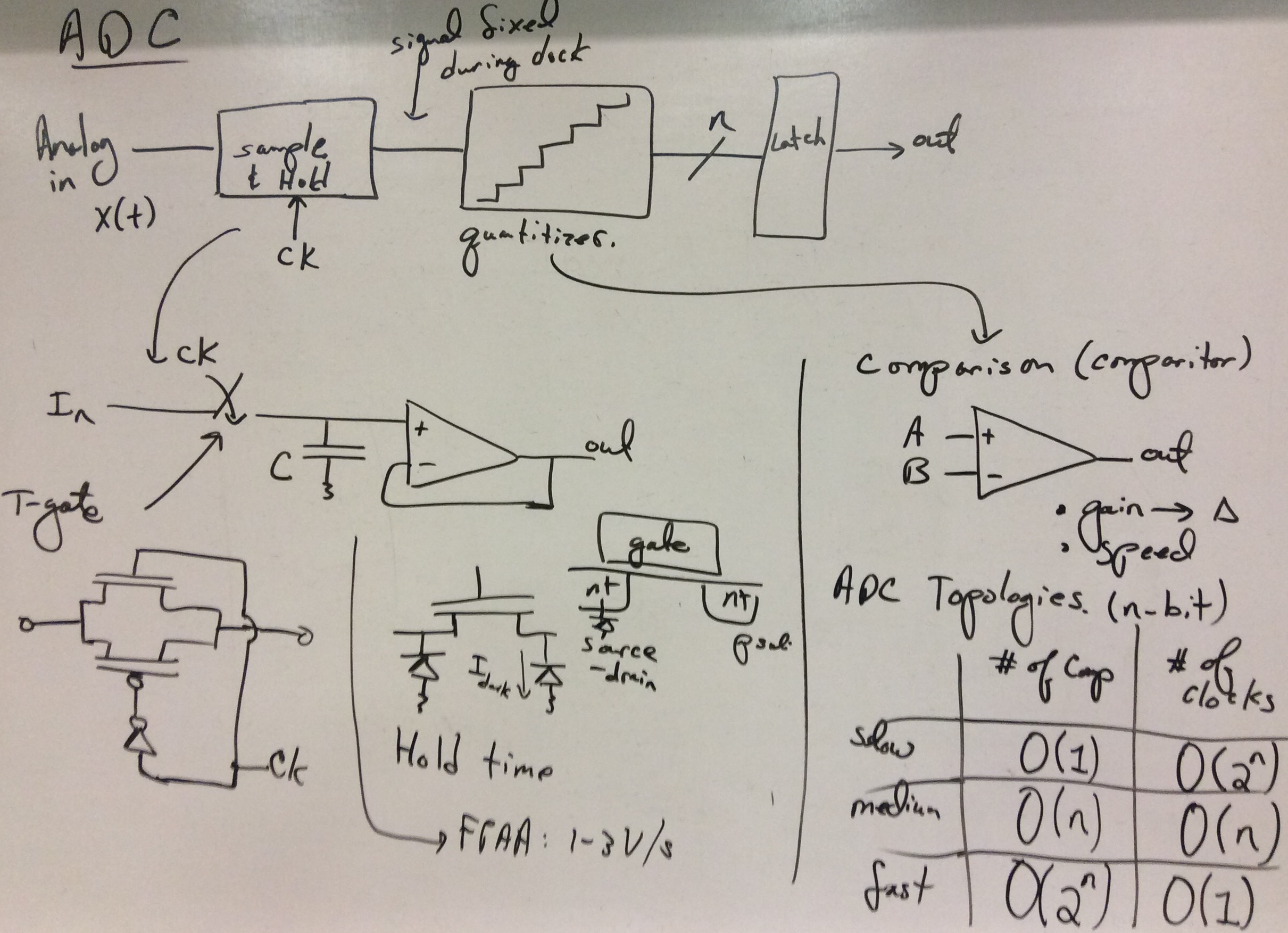
ADC Stage:
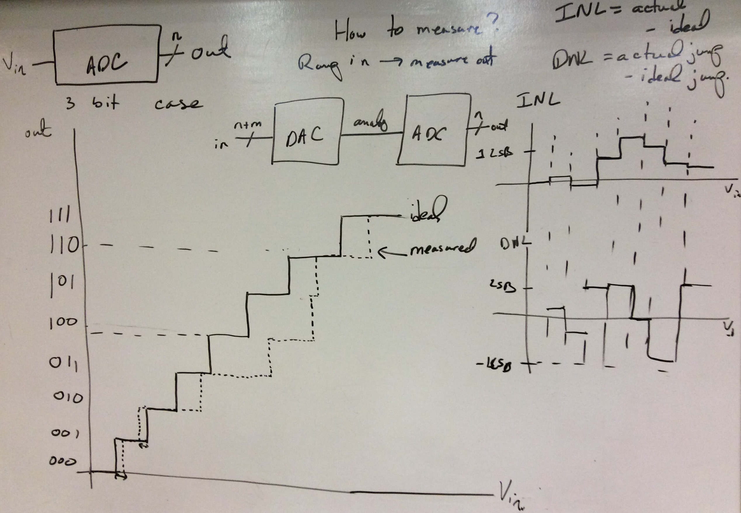
The ADC computation must be able to take a signal
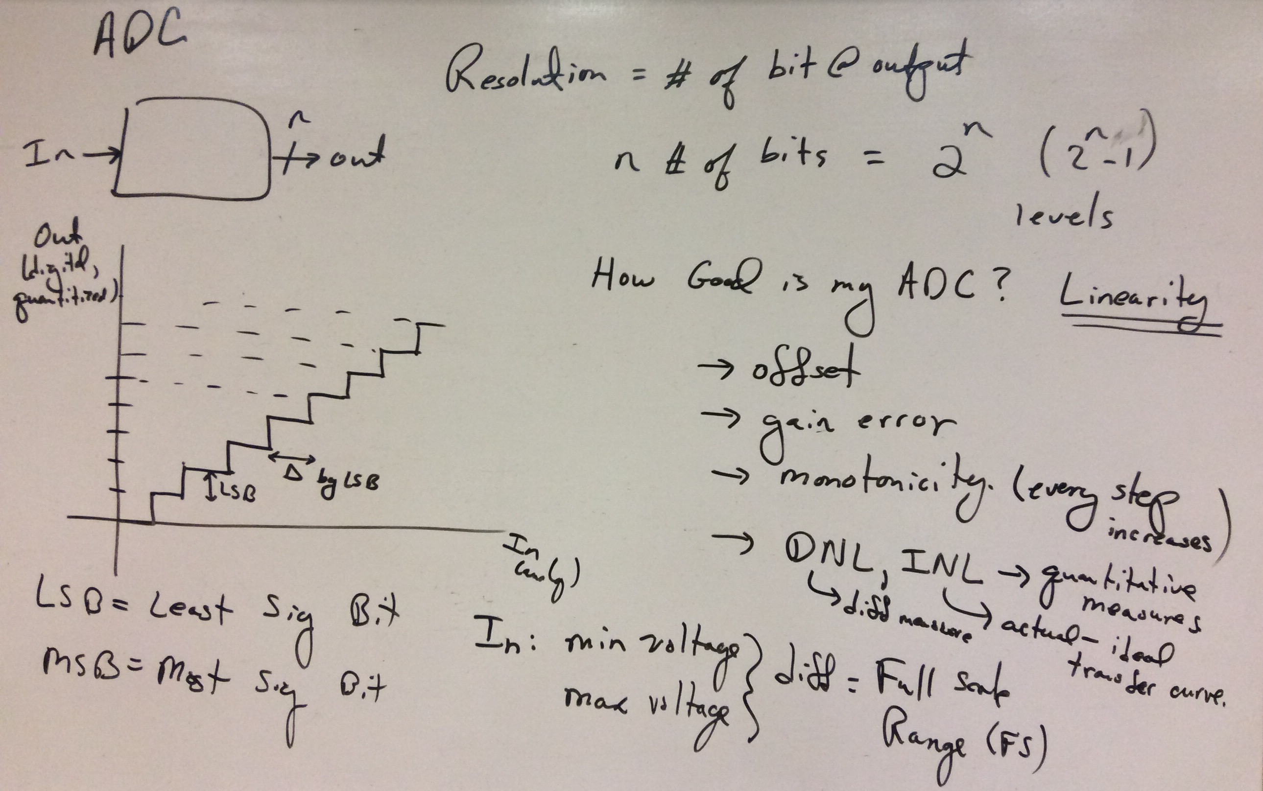
in the range from 300mV to 2.2V and convert it to the desired resolution;
10bit resolution and linearity for the faster channel, and
16bit resolution and linearity for the slower channel.
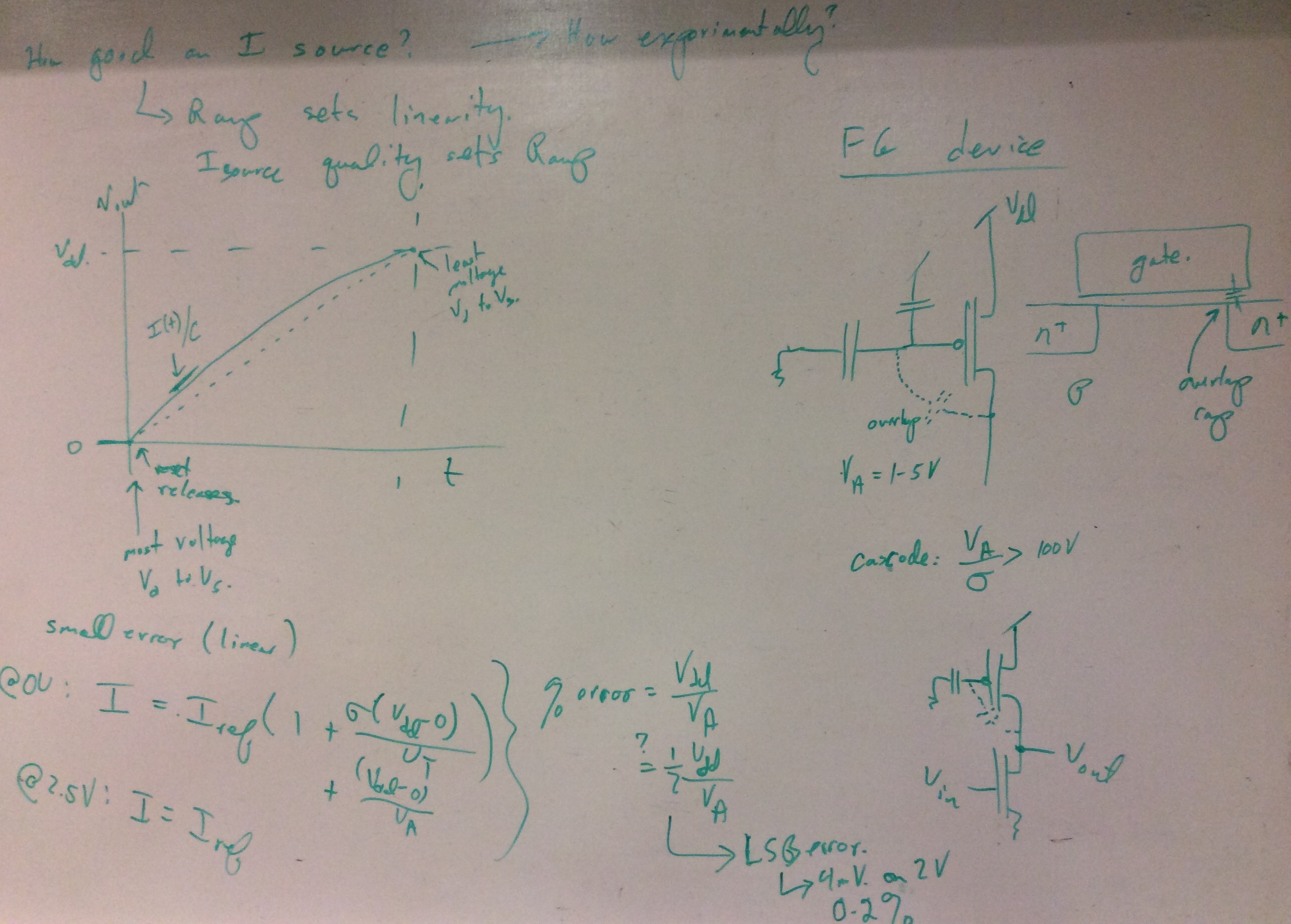
Linearity should be demonstrated in terms of INL and DNL measurements at the maximum frequency of the ADC operation.
Other related approaches would be useful (i.e. frequency response with noise and nonlinearities),
although it could require significantly more simulation time.
We expect both of the filters to output a signal that is maximum at 2V peak to peak in the power supply. The signal must be away from the power supply rails by 300mV.
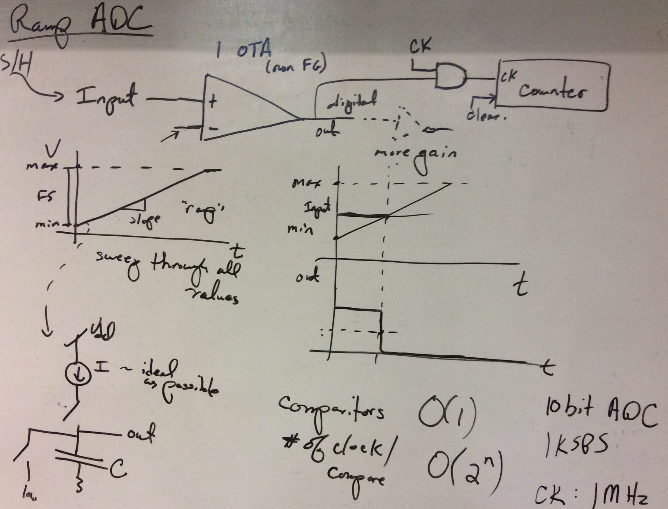
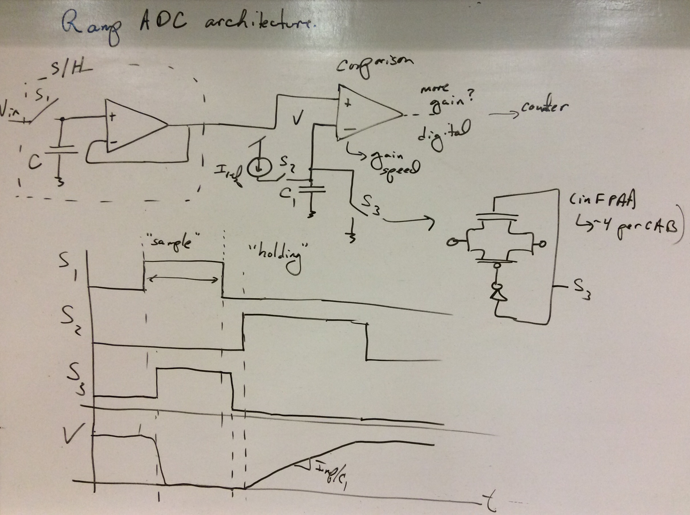
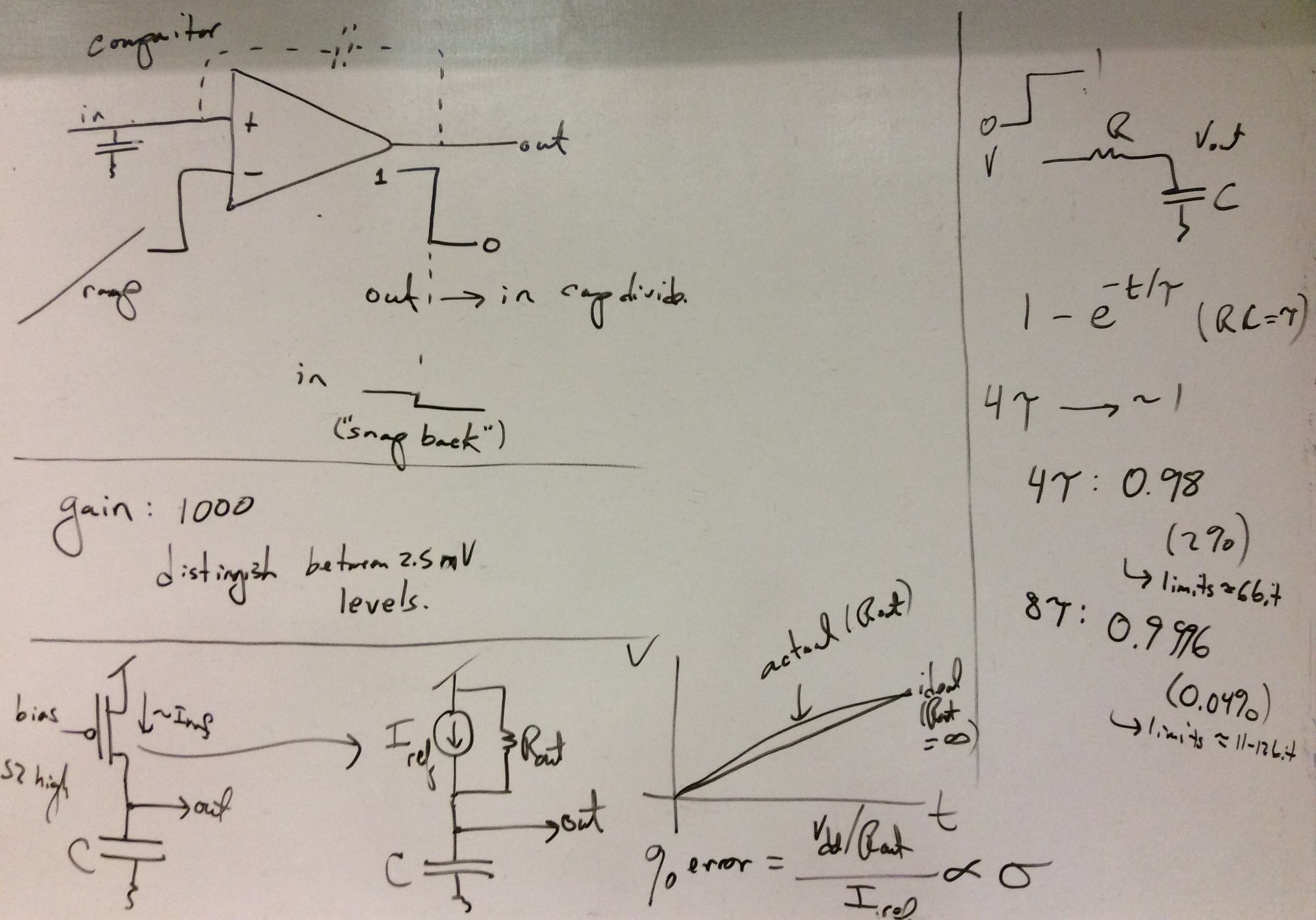
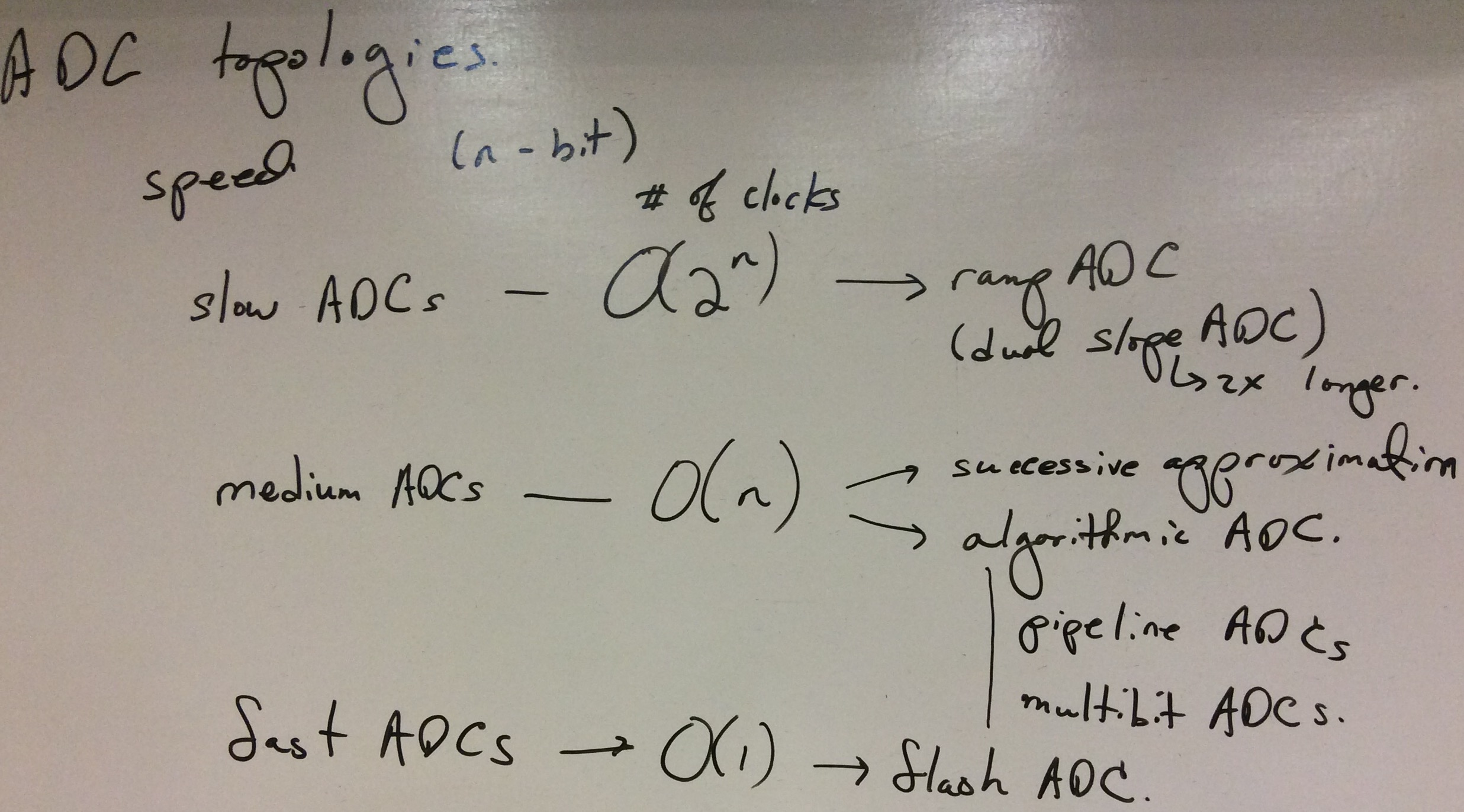
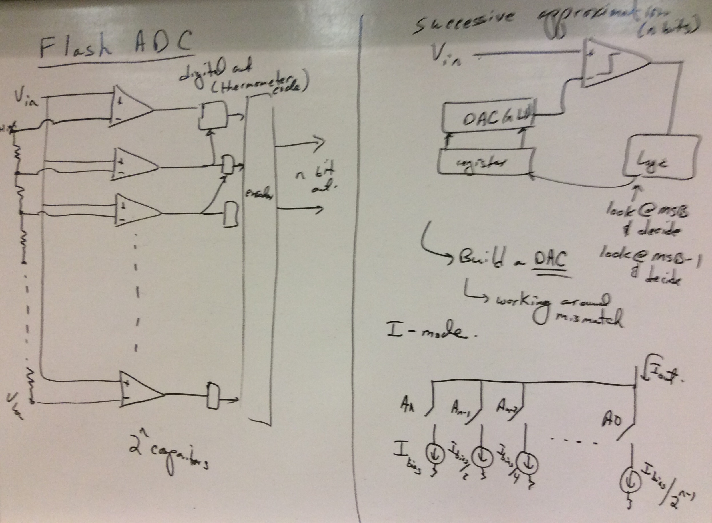
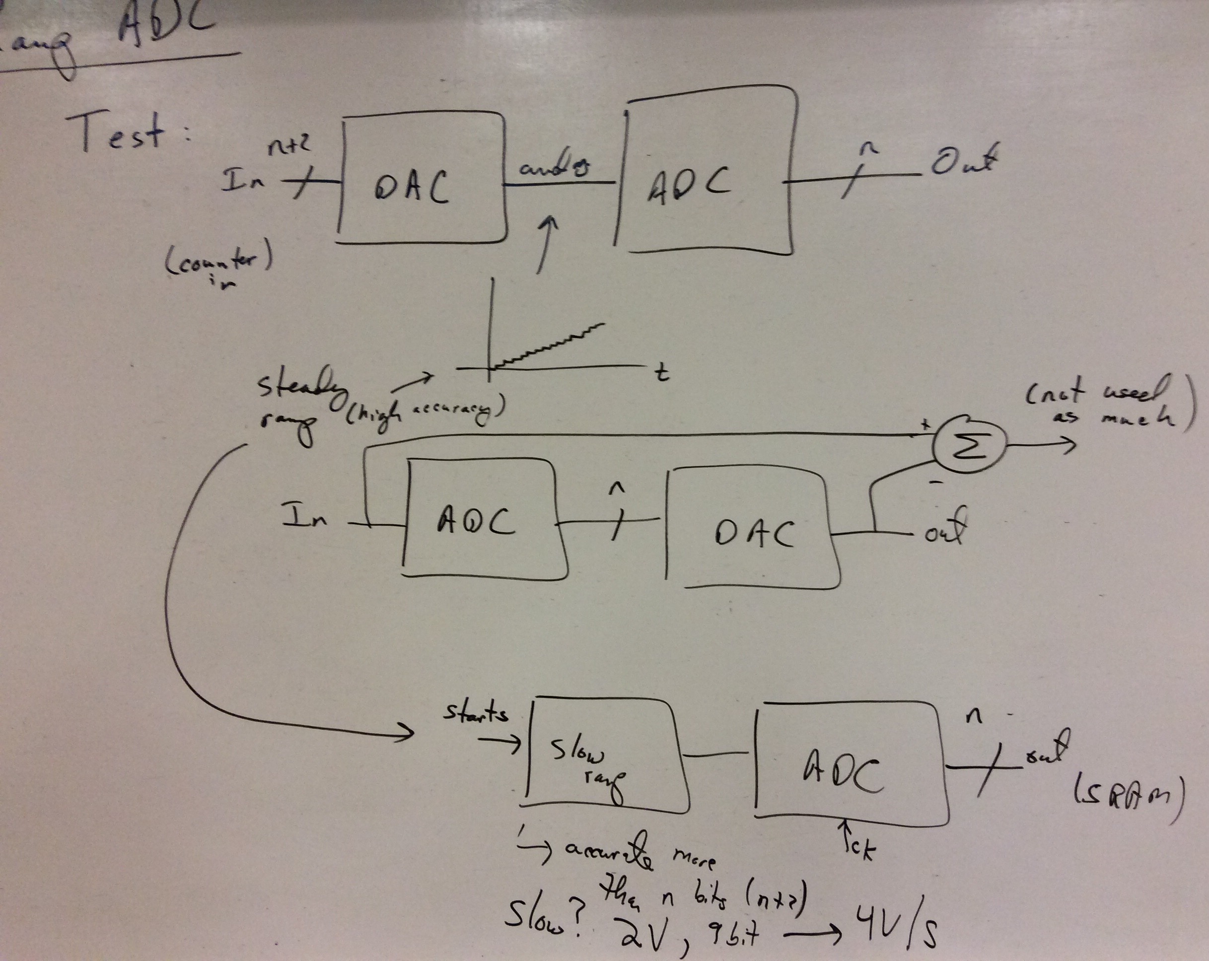
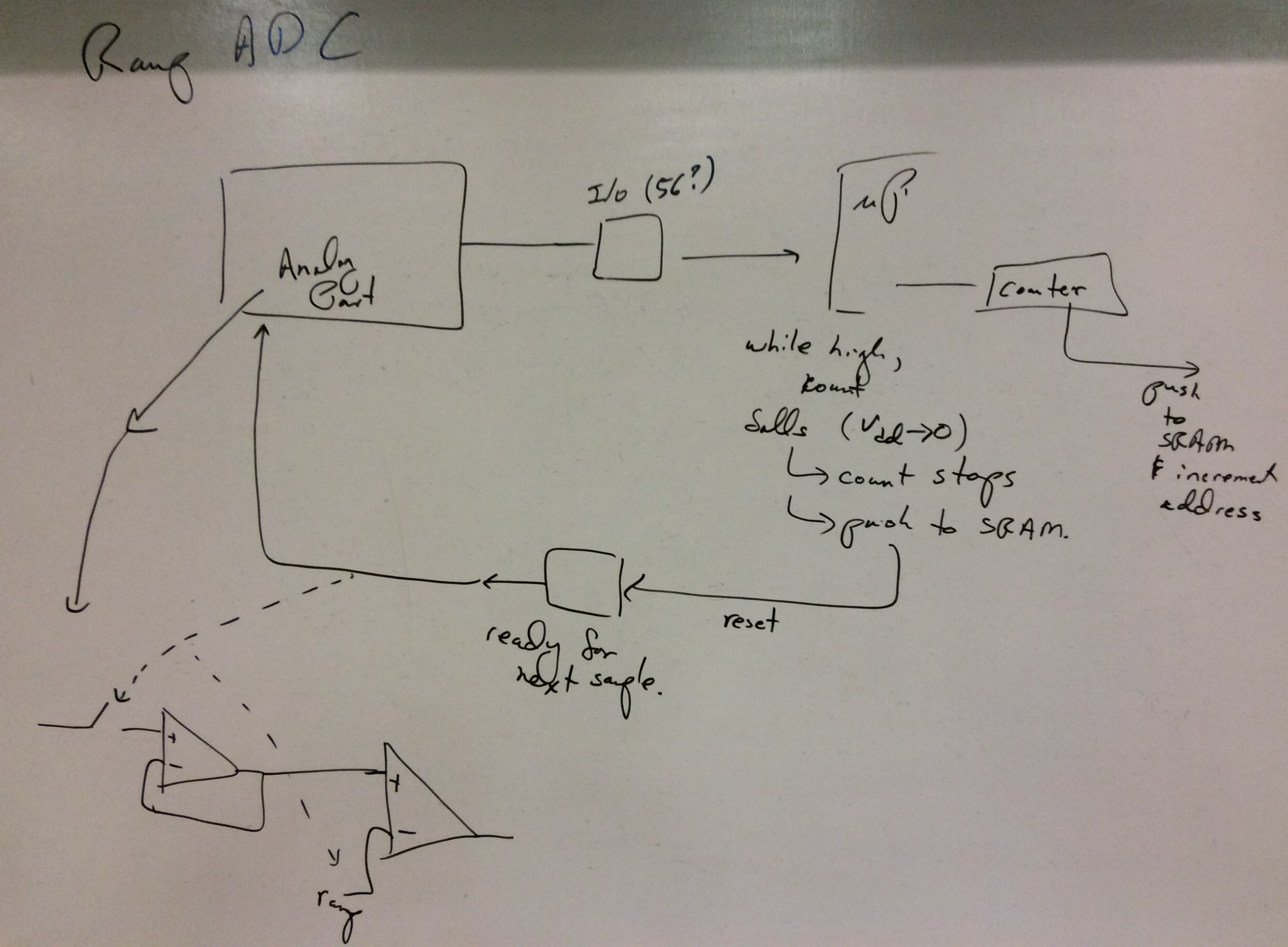
One would expect the low speed, 16bit ADC would be a single-slope or dual-slope ADC, given the low sample frequency requirement.
The higher speed ADC could be accomplished by a dual-slope ADC for the sample rate or by other approaches.
Fall 2016 Project requirements
For this project we will attempt to reach part of these specifications
for the neural measurement, particularly the faster neural measurement system.
Groups will be divided into two group types:
- Group type A will build the LNA + Filter stage,
- Group type B will build the ADC stage.
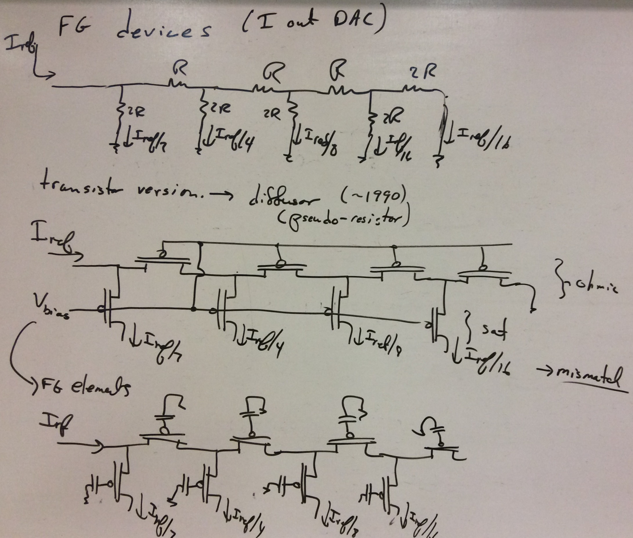
Everything will be built in the FPAA devices, and you can use any devices
available in the SoC FPAA device.
That includes all FG devices and all OTA devices.
Experimental data is essential.
Scilab/Xcos sim can be used to help illustrate,
but experimental data is required.
Outside simulation engines will not be accepted.
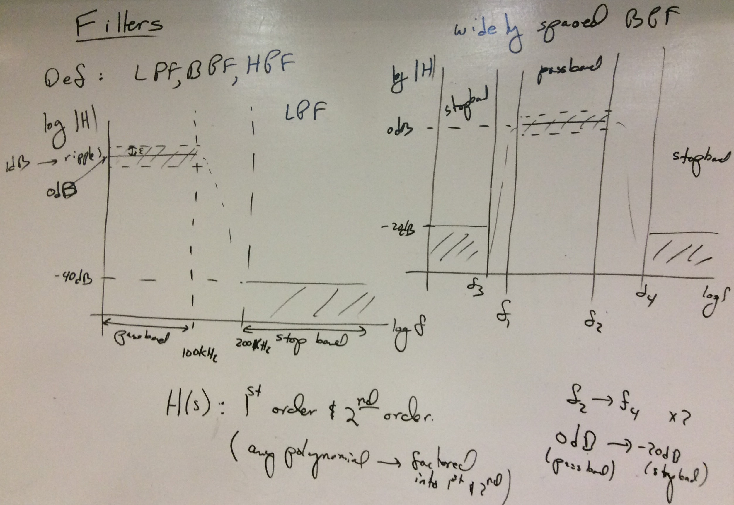
The specifications for the LNA + Filter stage
- Require 30dB of gain
- Filter stage (gain of 1)
with 8Hz to 250Hz passband (1dB ripple),
with -20dB down, 4Hz to 500Hz stopband
Your project can combine the LNA into the filter stage if helpful.
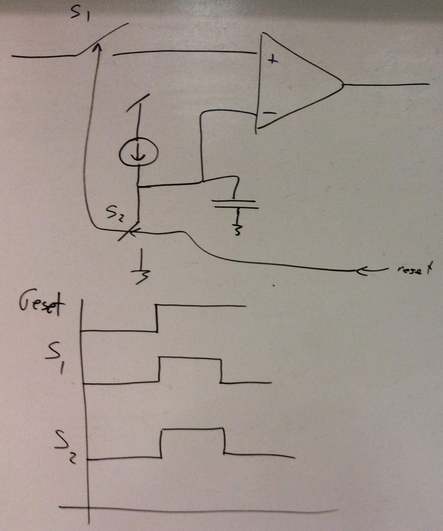
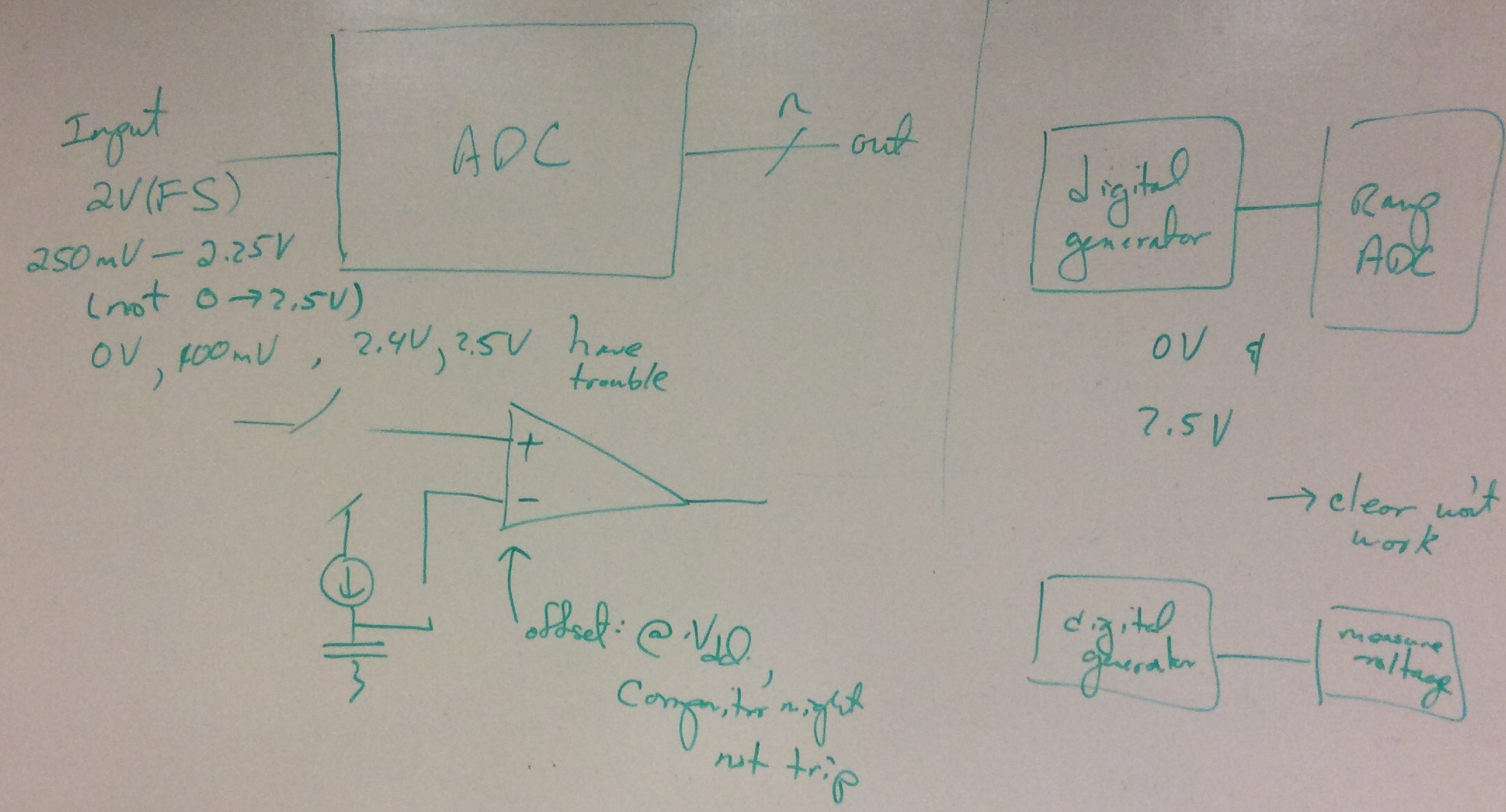
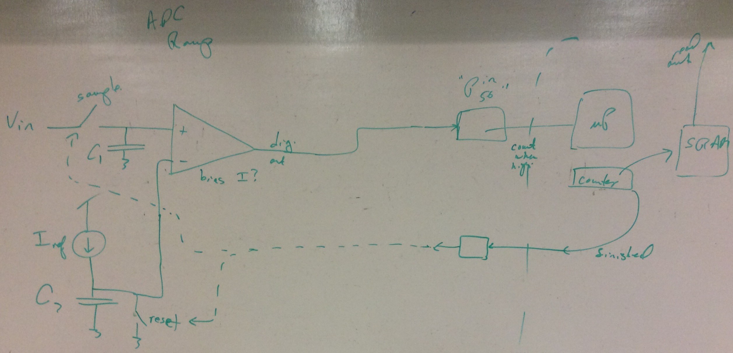
The specifications for the ADC stage
- 1kSPS sample rate
- 9bit linearity (INL, DNL)
- Full scale range =2V (250mV to 2.25V)
- probable implementation will be a dual-slope ramp ADC,
although others are possible
Application 2: Front-end for an Ultrasound sensor used in a pulse echo sensing
Figure 1
shows the block diagram for an analog system for an Ultrasound sensor used in a pulse echo application.
Such approaches are used by having a separate device or devices send out an ultrasound wave,
that will reflect from the moving target (or flow of a target),
and return with a particular delay.
Ultrasound starts at frequencies above human hearing, like 40 to 60kHz, and can reach beyond 30MHz.
The frequency used is inversely related to the spatial resolution;
lower frequencies are good for sensing longer distances,
and higher frequencies are good for sensing short distances.
For this problem, we will consider a mid-range application where we might be wanting to monitor the flow of people
(number of people, average crowd velocity) through a particular
building hallway or outside passageway, say like at an amusement park.
For this application, we would want a frequency of 80kHz as the primary driving frequency.
The signal will typically attenuate through the atmosphere, so we expect our transmitted signal,
which is roughly a 1V transmitted sinusoidal 80kHz signal (a lot more on impedances, etc, but not to worry here),
resulting in a signal in the range of 30mV to 1mV (or less if no one is there),
although signals could get as high as 100mV in rare cases (someone walking near the transmitter)
LNA stage:
For the ultrasound sensor, the input is a capacitive input from two plates operating in air.
The job for the LNA is to take this capacitive input,
which could be maximum of 5 percent change of the total 1pF capacitance,
to have a signal with reasonable dynamic range.
Realize that the capacitance of the bonding wire / pad to the sensor would be 5pF.
One approach would be to read the AC coupled signal as a result of this capacitive divider, which would be attenuated by the capacitive divider.
These approaches would require having an amplifier with at least 30dB of gain, just to get a reasonable signal at the output.
A 5 percent change on a 2.5V supply would be a 20mV input to the next stage.
With the resulting signal attenuation from transmission of -20dB in the best case, one would want roughly 50dB of gain in this case.
One must also assume that the environment will change the resulting dc potential of this incoming signal,
so we should assume the input signal is AC coupled.
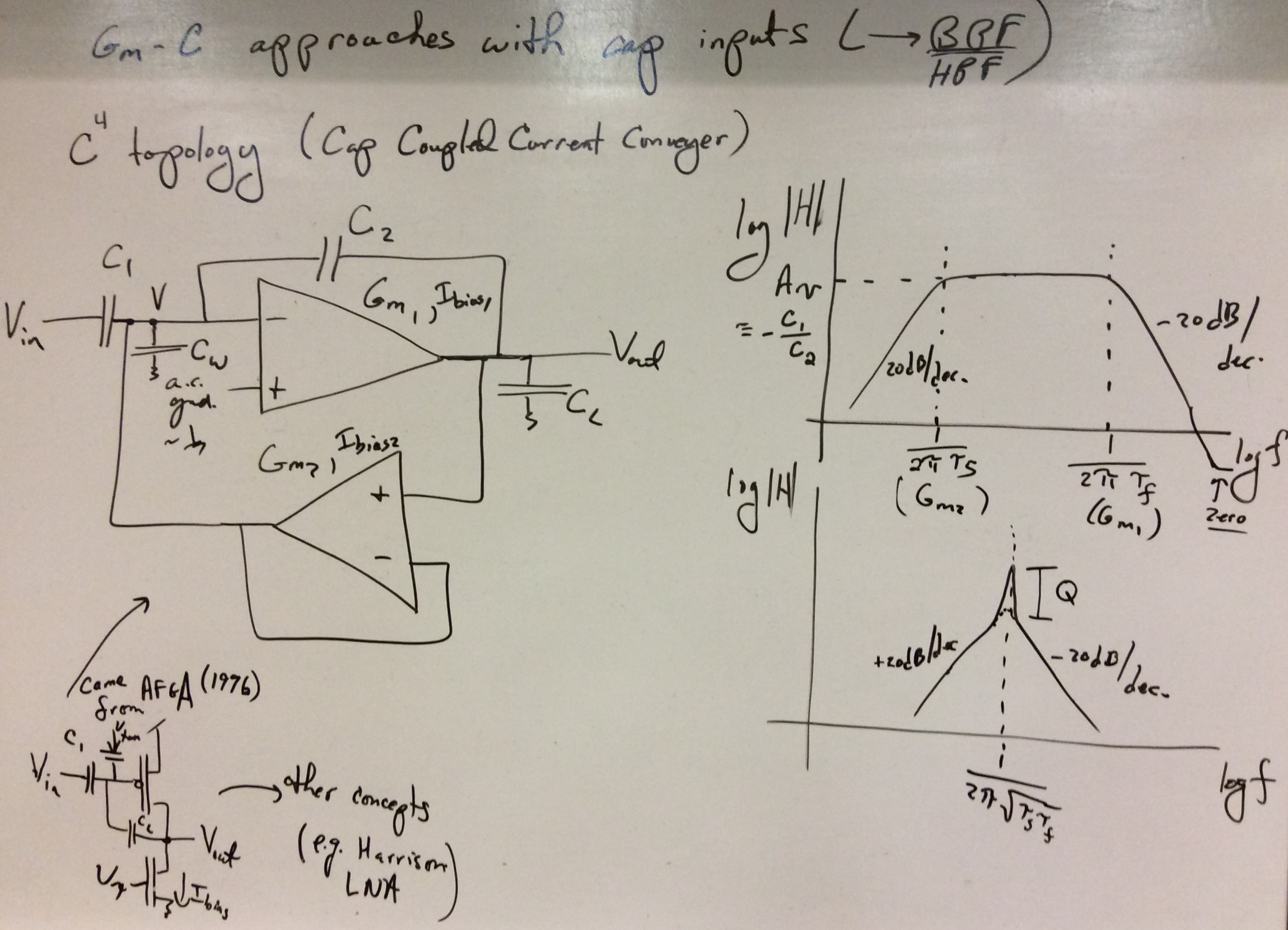
The other approach would be to use an amplifier that directly senses the capacitance, using capacitance in an amplifier feedback loop.
One paper in the list is a classic paper on capacitive amplifiers which should help the resulting design.
We expect the output signal into the next stage is a peak of 100mV,
with the output SNR of this stage being 60dB.
Filter stage:
We will be interested in signals that are in the 70kHz to 90kHz band and wanting to attenuate signals outside of this region.
We are interested in the frequency spectrum in terms of potential frequency shifts due to moving objects.
The stop band must be -20dB down at 60kHz for lower frequencies and -20dB down at 100kHz for higher frequencies.
We expect a maximum change of 1dB ripple in the passband.
Distortion for a 100mV input sinusoidal signal in the band of interest should be at least -34dB below the primary harmonic for a two-tone test.
The SNR needs to be 54dB SNR from the output filter.
We expect both of the filters to output a signal that is maximum at 2V peak to peak in the power supply. Remember the peak input voltage would be expected to be 100mV.
You should not expect the output to be a known dc voltage, but rather will have to handle that issue.
Since you are making a bandpass filter, the dc is not important in the computation, and should not be a difficult specification.
The signal must be away from the power supply rails by 300mV.
ADC stage:
The ADC computation must be able to take a signal in the range from 300mV to 3V and convert it to
10bit resolution and linearity
at a sample rate of 200kSPS.
We have stretch goal of reaching 12bit linearity and resolution,although that goal will be rather aggressive to accomplish.
Linearity should be demonstrated in terms of INL and DNL measurements at the maximum frequency of the ADC operation.
Other related approaches would be useful (i.e. frequency response with noise and nonlinearities),
although it could require significantly more simulation time.
At this sample rate, a single or dual slope converter will be rather aggressive, requiring a counter running at 200MHz (for 10bit), although could be possible.
One might also find a converter approach such as successive approximation, or an algorithmic ADC convertor, might be an easier solution for the convertor.
Additional Materials on IC system design
- Documentation on working with digital counter
on SoC FPAA structure
- Thoughts on using the remote
system
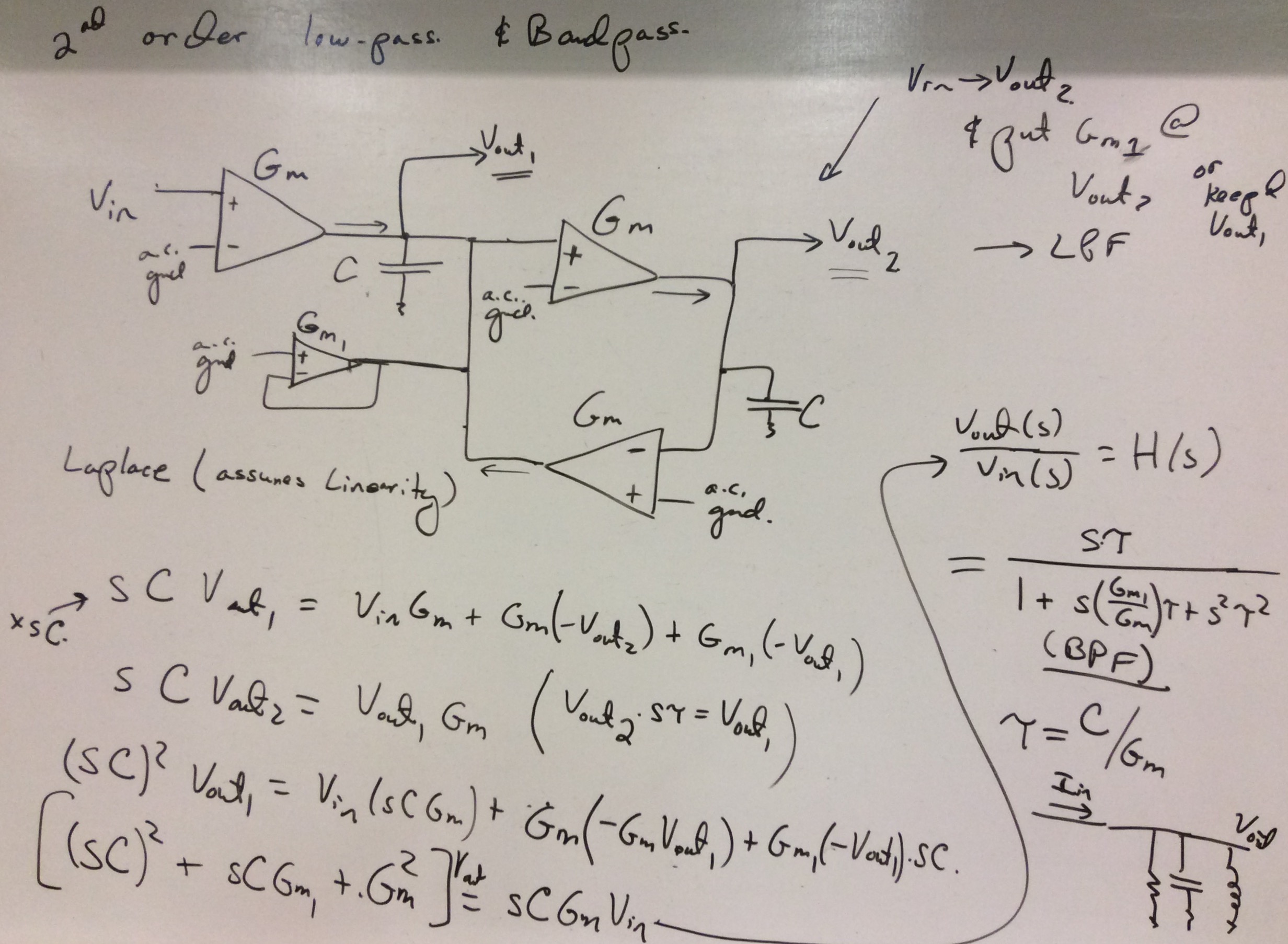
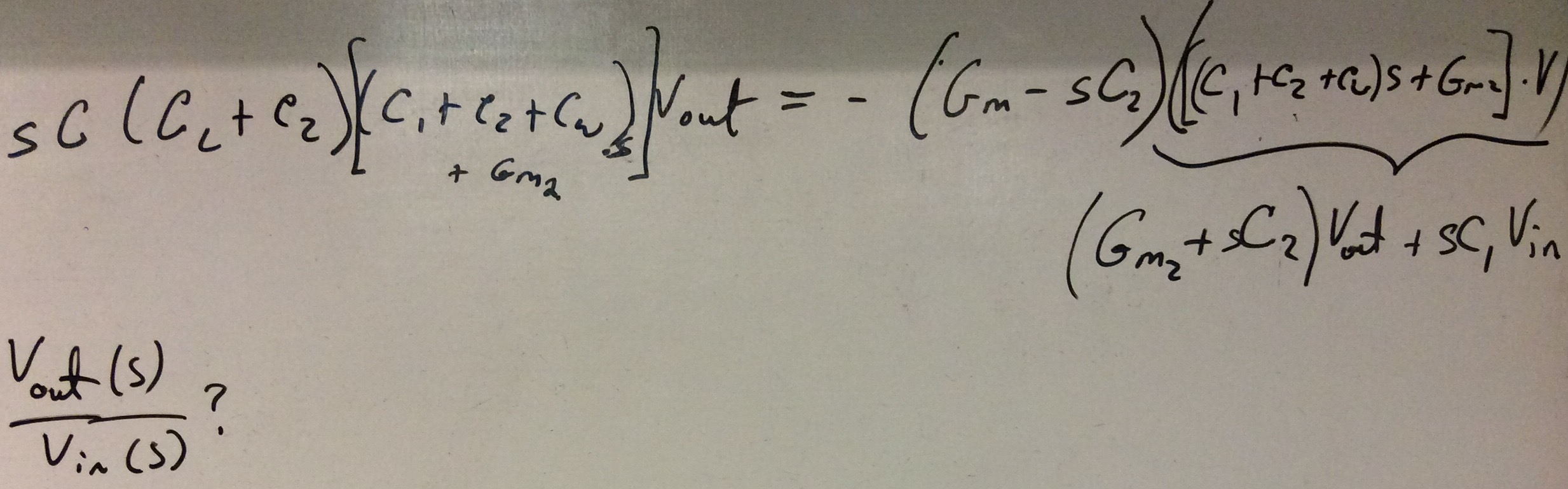
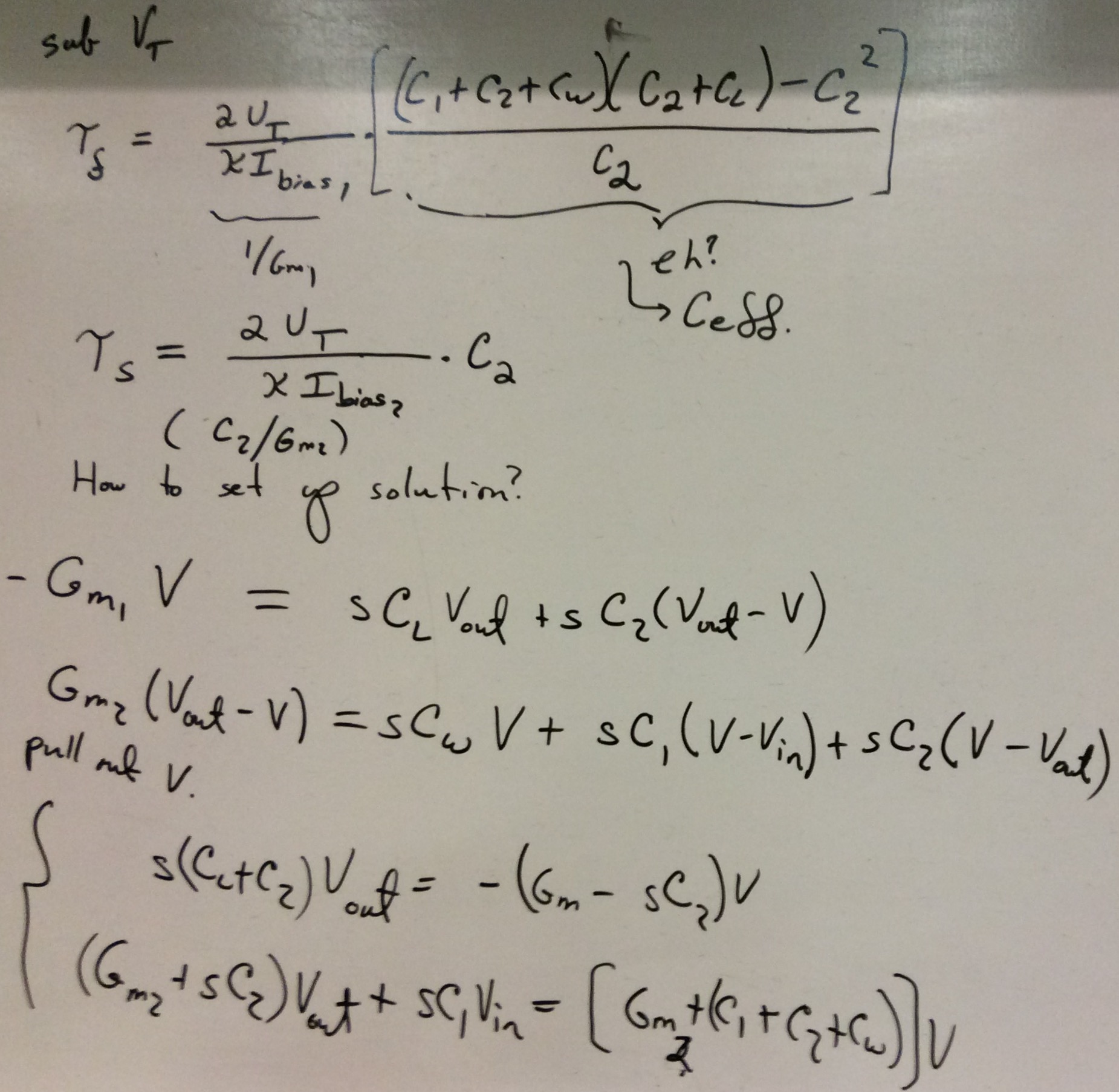
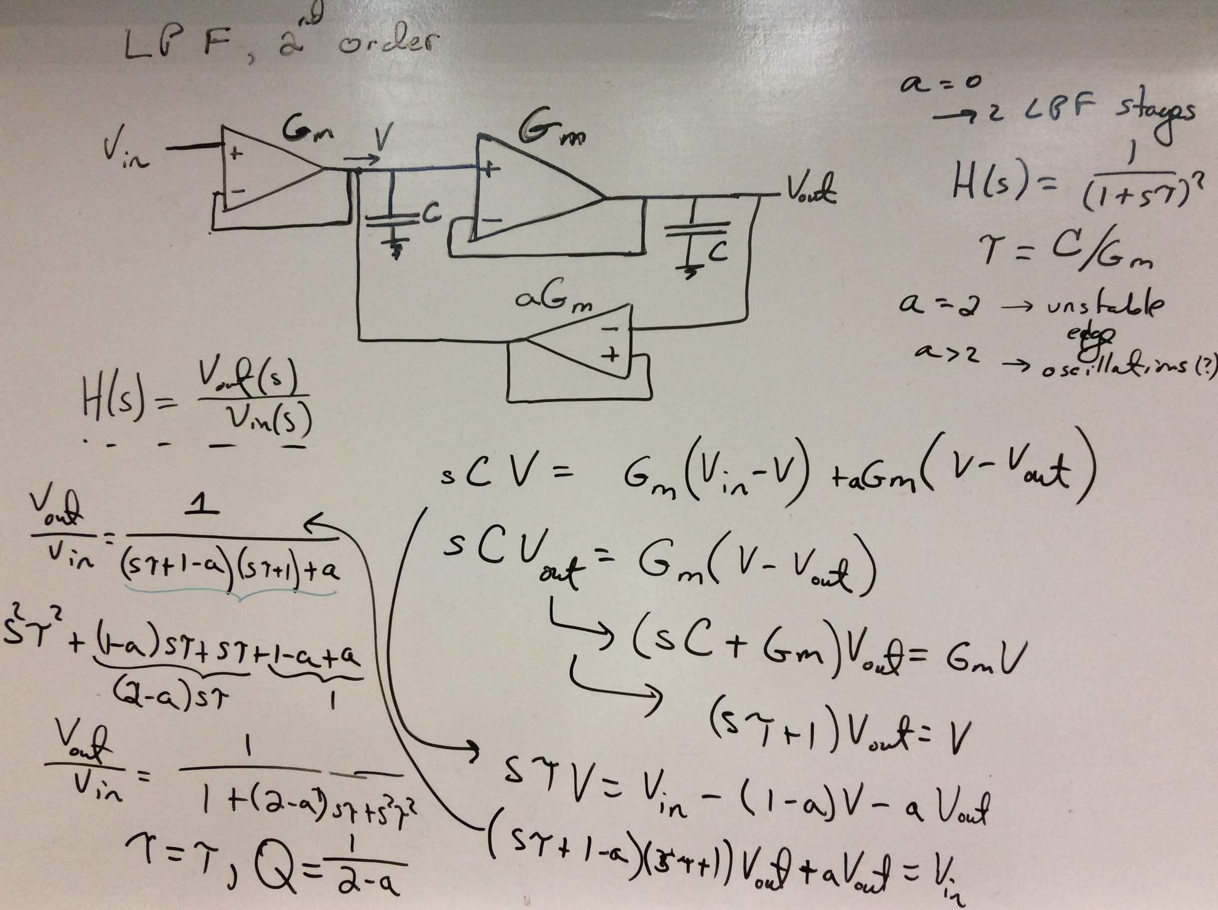
- Notes on basic Filter
architecture .
- Notes on fundamentals of capacitor
circuits
as well as basic switched capacitor
circuits .
- Notes on basic sample and hold
circuits .
Further, we include the classic two papers
on charge feedthrough modeling
pdf ,
and
pdf .
- Notes on starting point for comparitor
circuits .
- Notes on basics of Data Converter
circuits ,
on Digital to Analog Converters (DAC)
circuits ,
and on High Speed Analog to Digital Converters (ADC)
circuits .
Outside Resources that might be useful
- Overview slides from TAMU on Sample and Hold
blocks
- Overview notes on Continuous-time Filter approaches at UC Berkeley
blocks
- Overview notes by G. Temes (OSU) on Continuous-Time Active Filters
blocks
- Overview notes on Switched Capacitor Filter approaches at UC Berkeley
blocks
- Overview notes on Switched Capacitor approaches at U of Calgary
blocks
- Overview talk by David Narim when he was working at ADI,
pdf ,
and gave this presenation at GT at that time.
Some items for review
- Classic paper on the design of a MOSFET amplifier
- Classic paper on the neural amplifier front-end circuit
- Classic paper on noise in semiconductor devices
- Classic technical report on the EKV simulation model
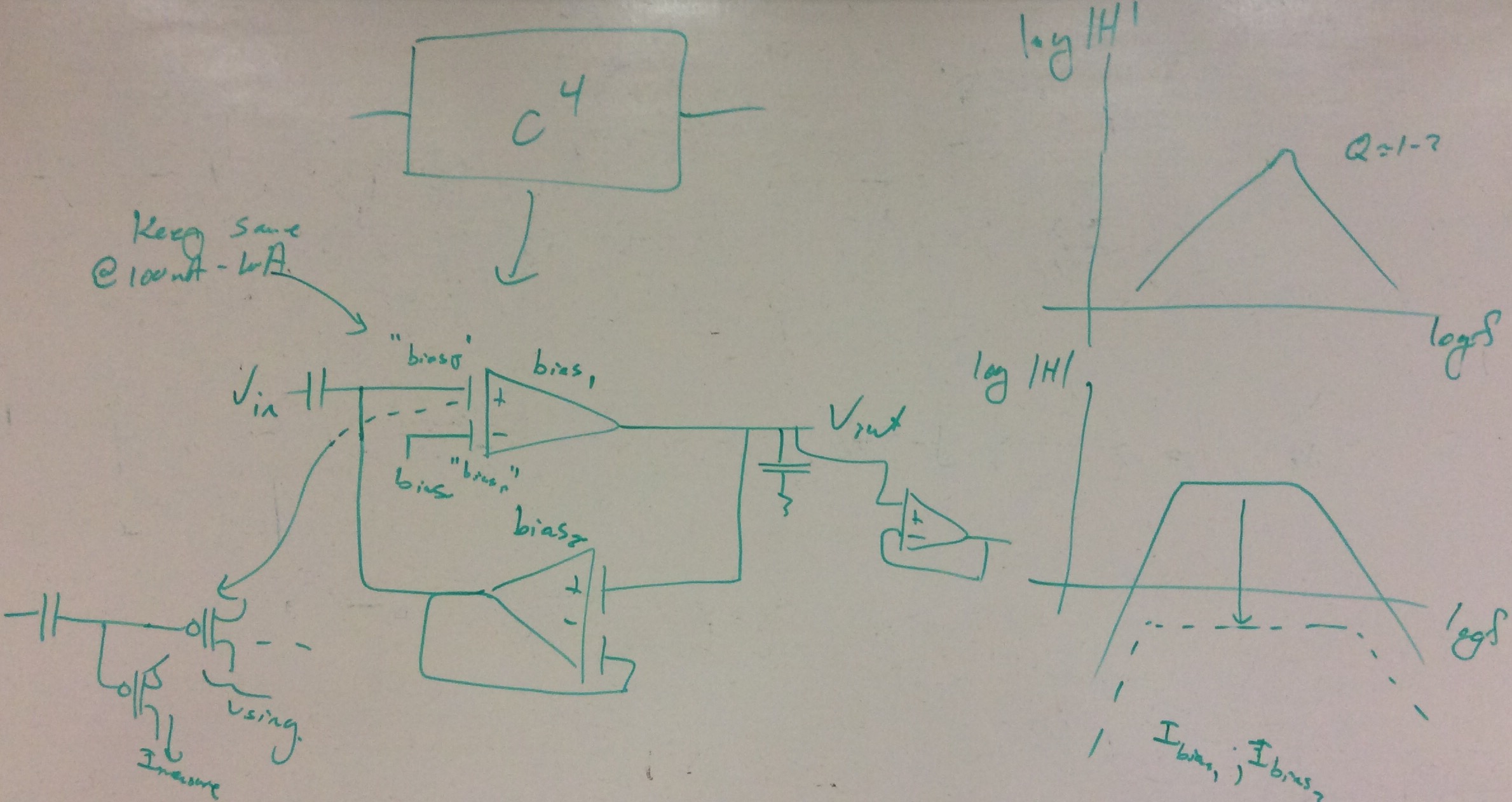
Lecture Boards
- Lecture on ADCs I:
1 ,
2 ,
3 ,
4 ,
- Lecture on ADCs II:
1 ,
2 ,
3 ,
4 ,
- Lecture on Filters I:
1 ,
2 ,
3 ,
4 ,
- Lecture on Filters II:
1 ,
2 ,
3 ,
4 ,
- Lecture on ADCs III:
1 ,
2 ,
3 ,
4 ,
5 ,
- Review Lecture on Project Concepts:
1 ,
2 ,
3 ,
4 ,
- Review Lecture II on Project Concepts:
1 ,
2 ,
3 ,
4 ,
5 ,