|
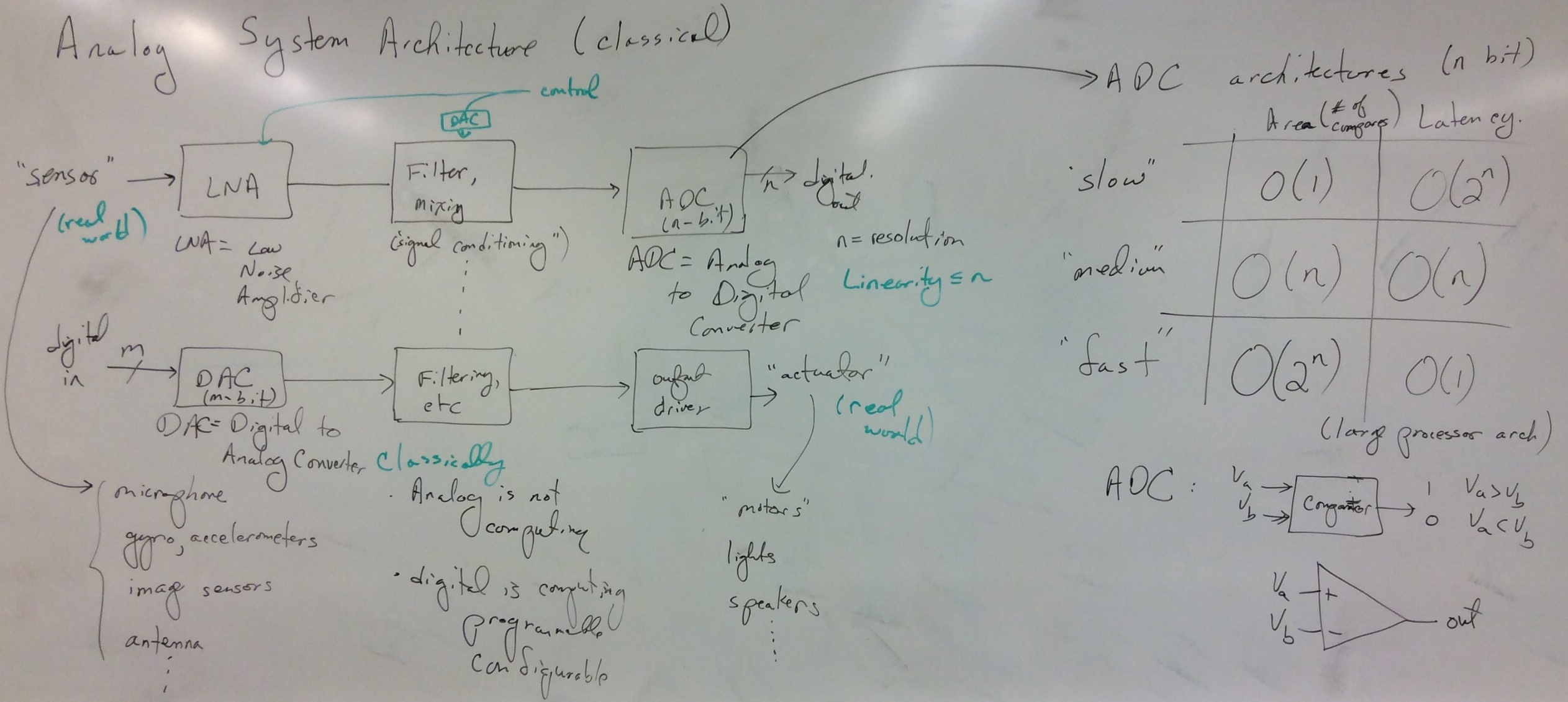
The focus on this fourth design project is to develop a design of an analog system. This project will utilize some of the component designs, as well as develop some additional component designs, towards building small analog system applications designed to be integrated with other analog components. Topics
Class Schedule and Video Viewing
Project is due Dec. 3. Project review requires each of the six groups to give a short (e.g. 7 minute) discussion about their current project design. Materials on IC system design
Outside Resources that might be useful
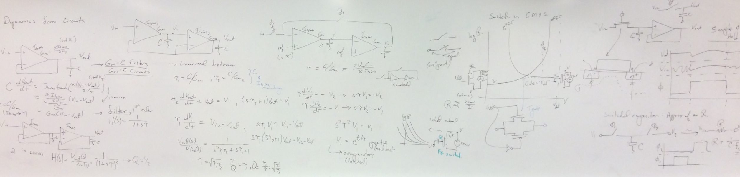
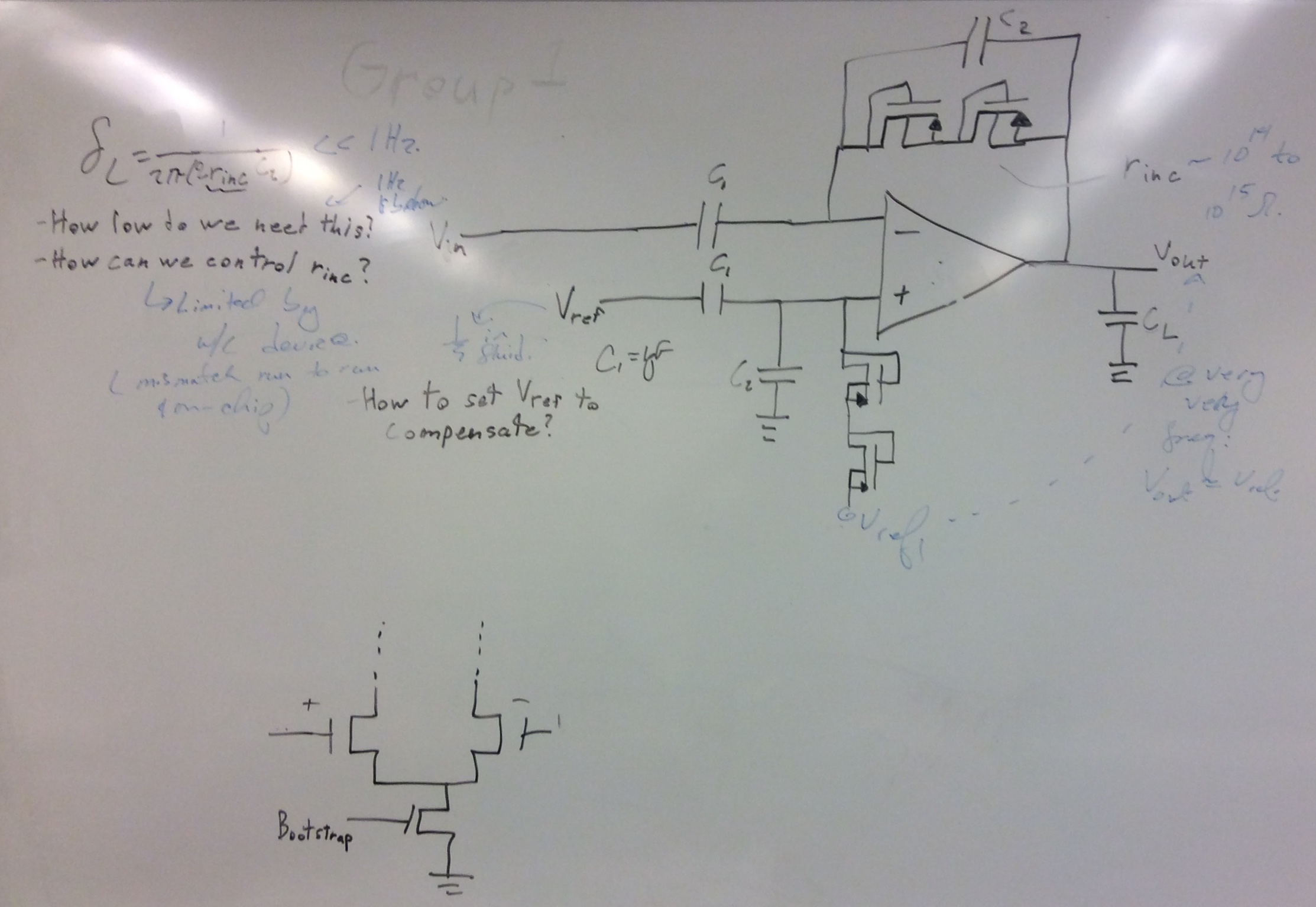
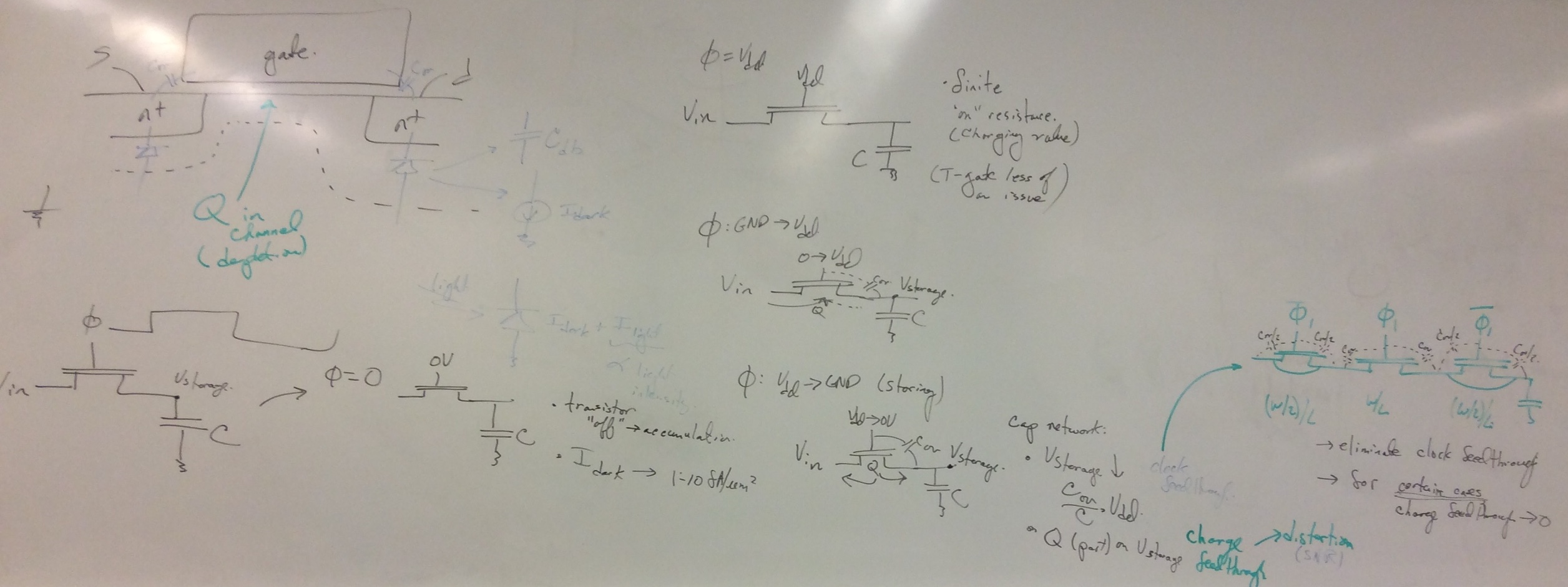
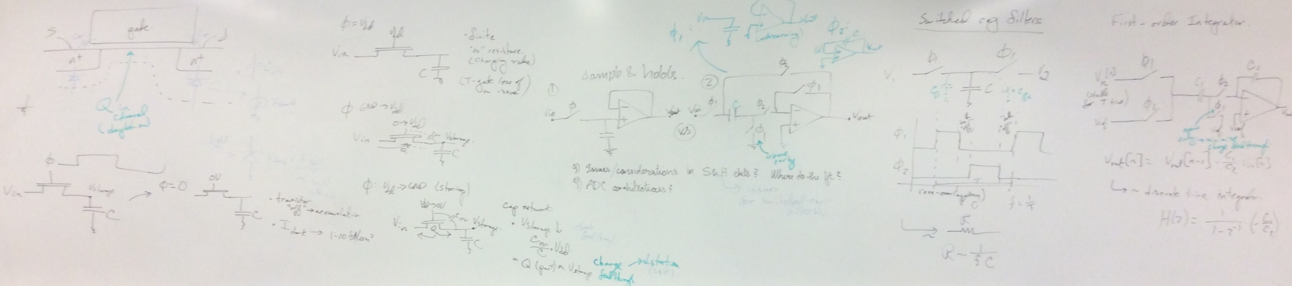
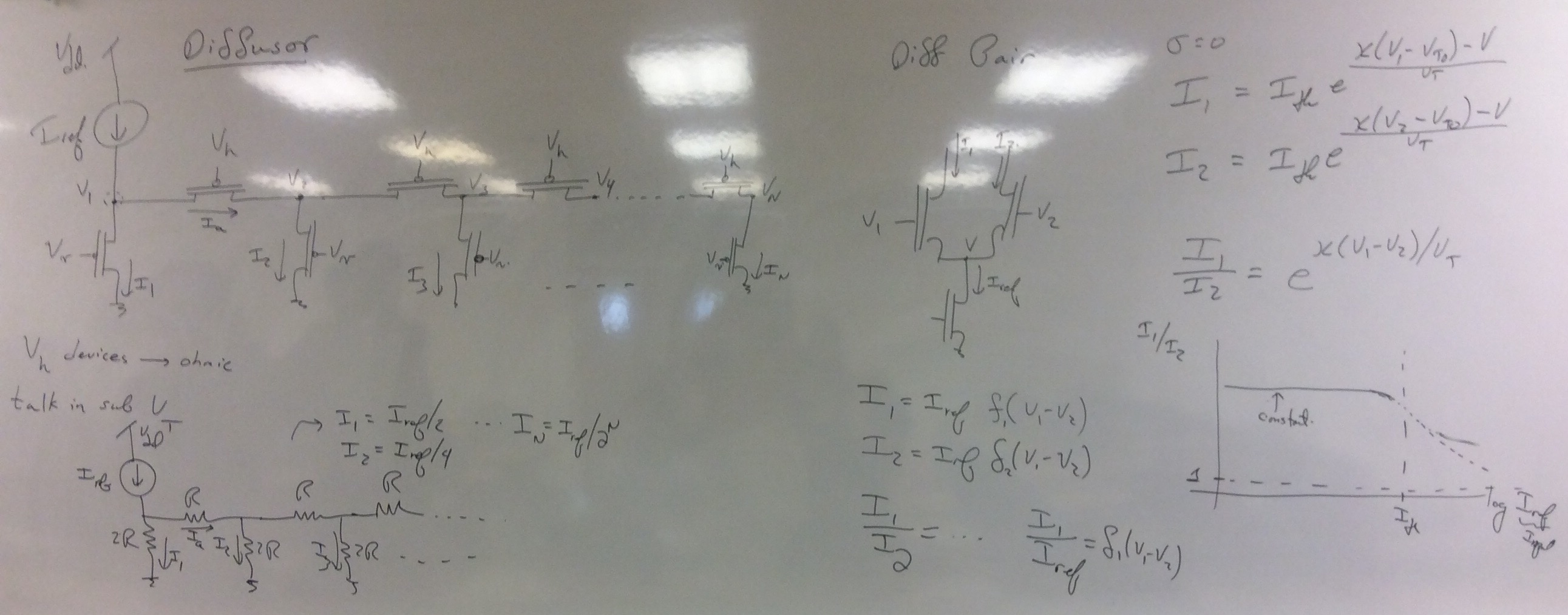
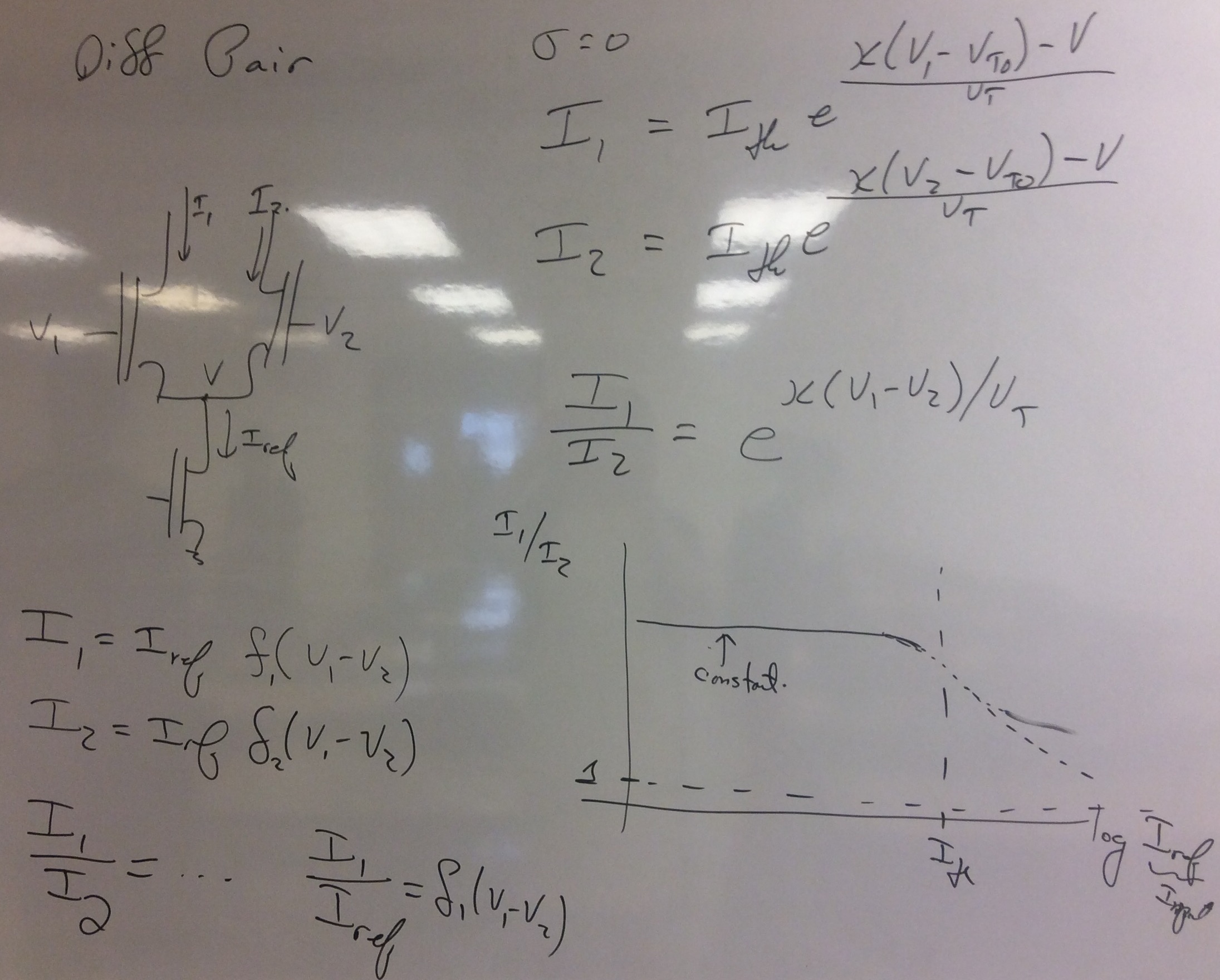
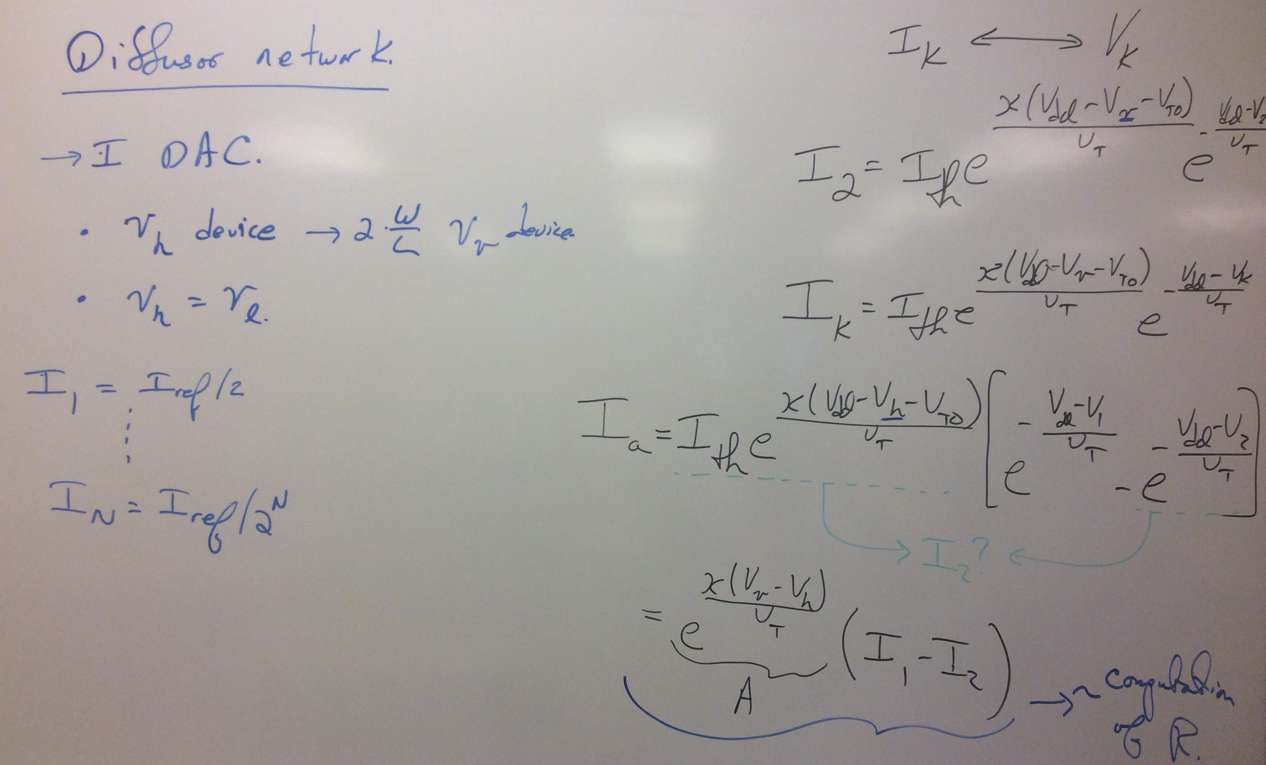
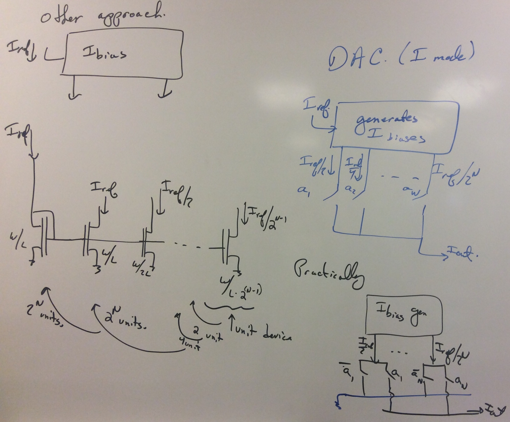
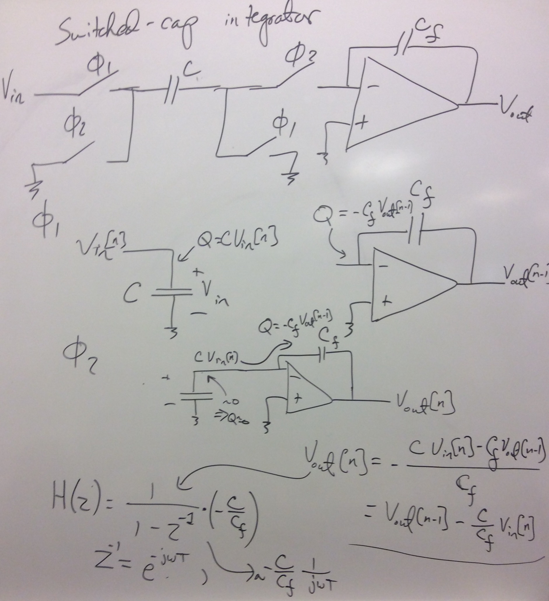
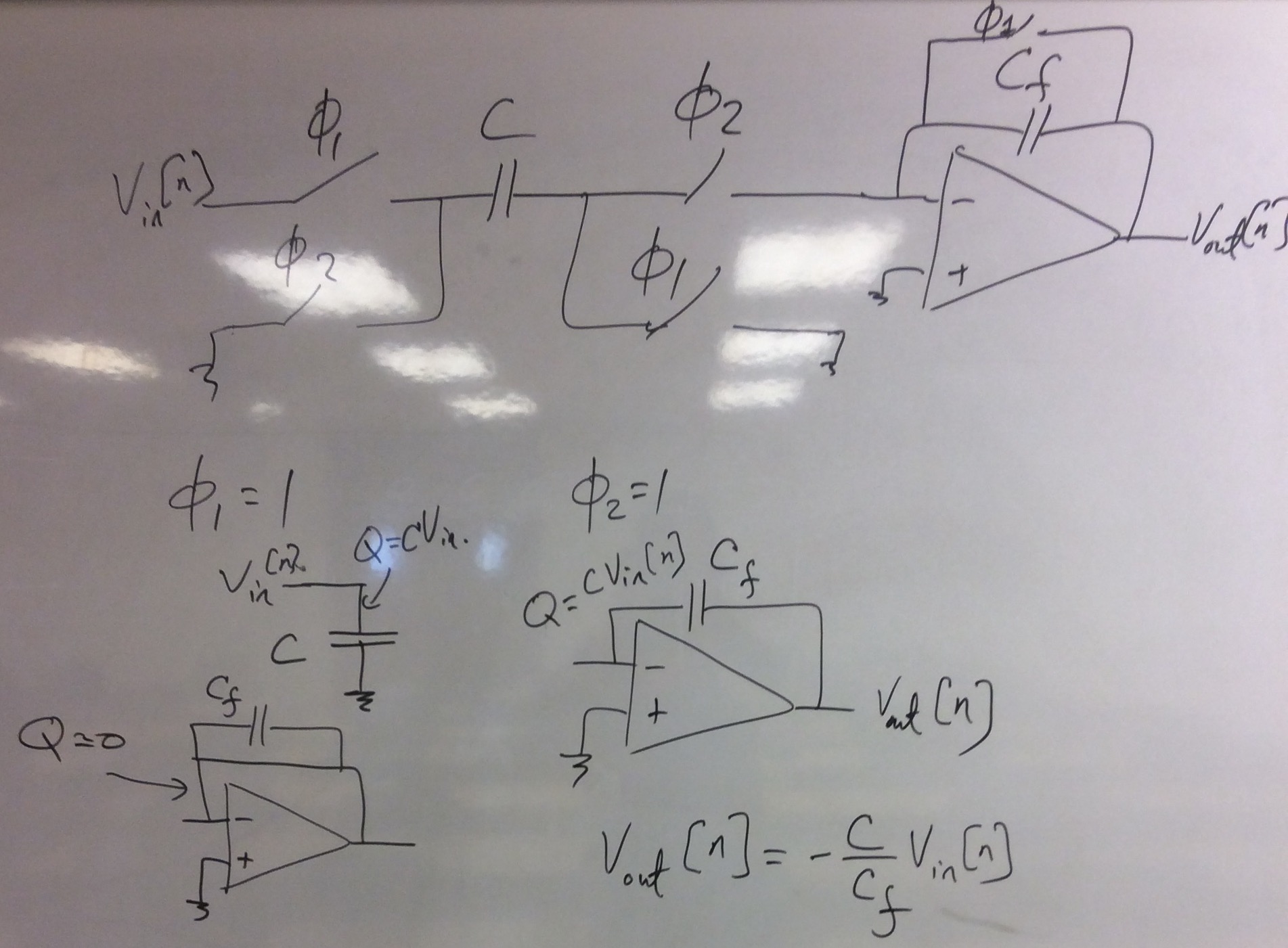
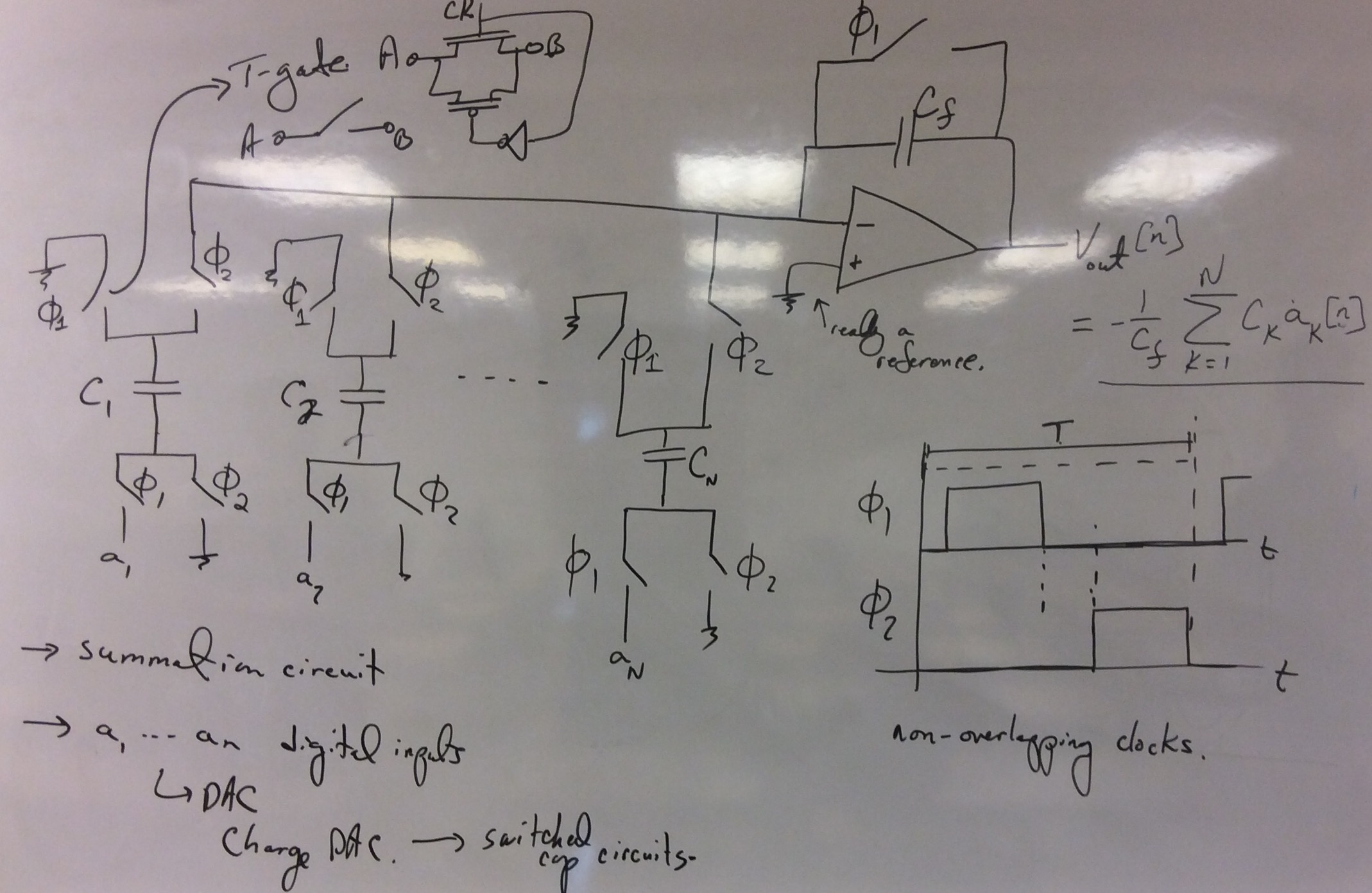
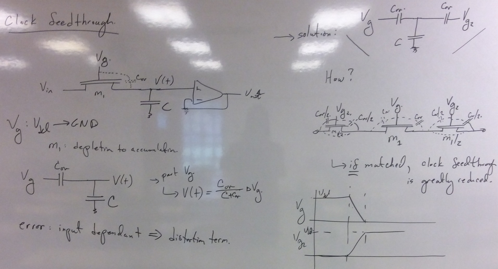
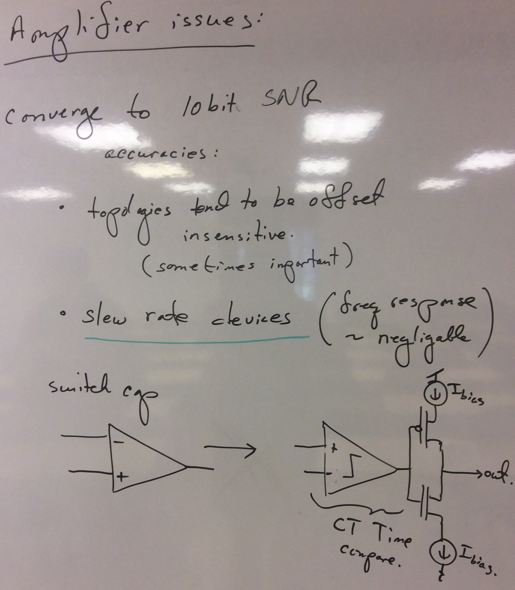
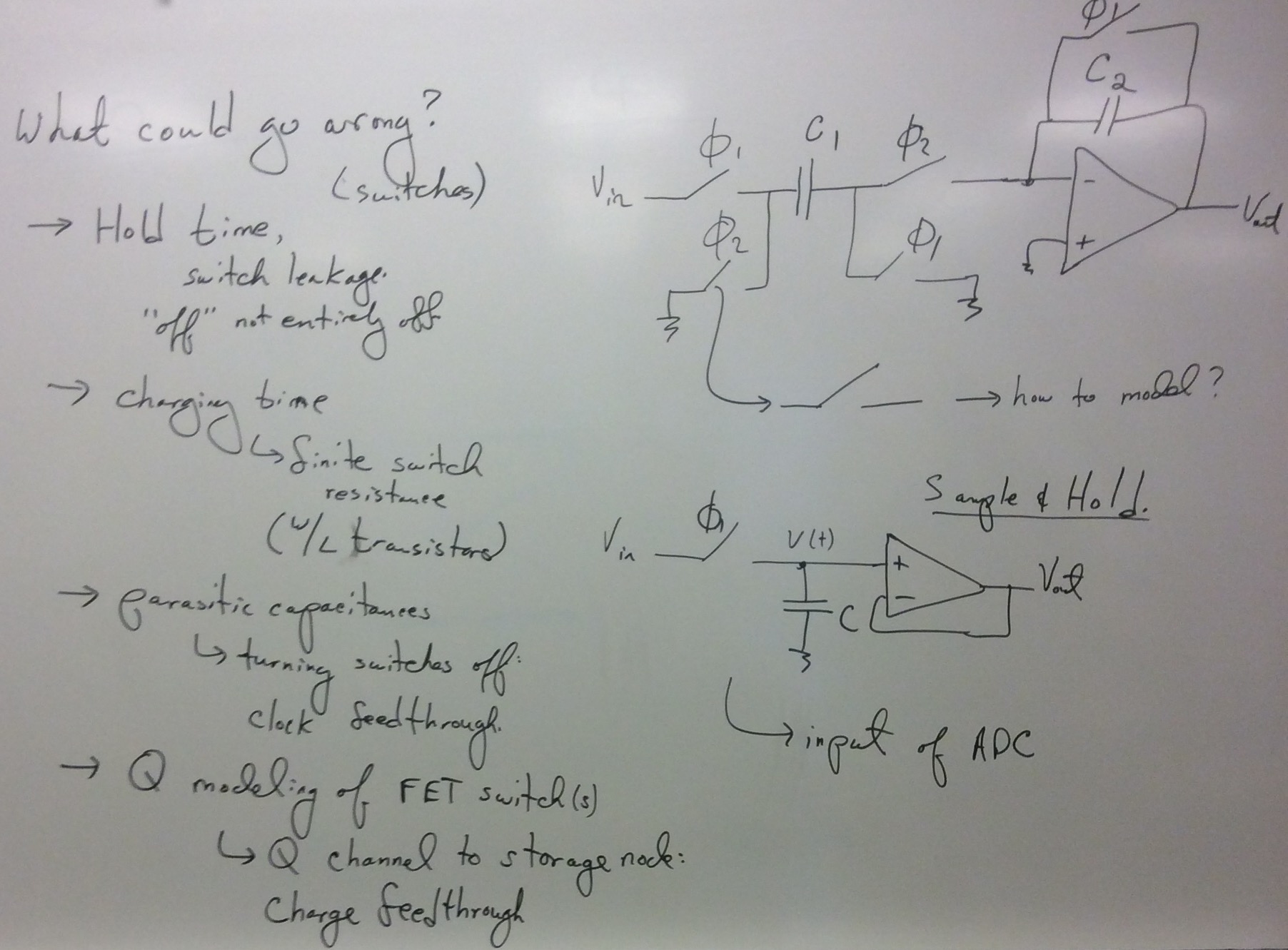
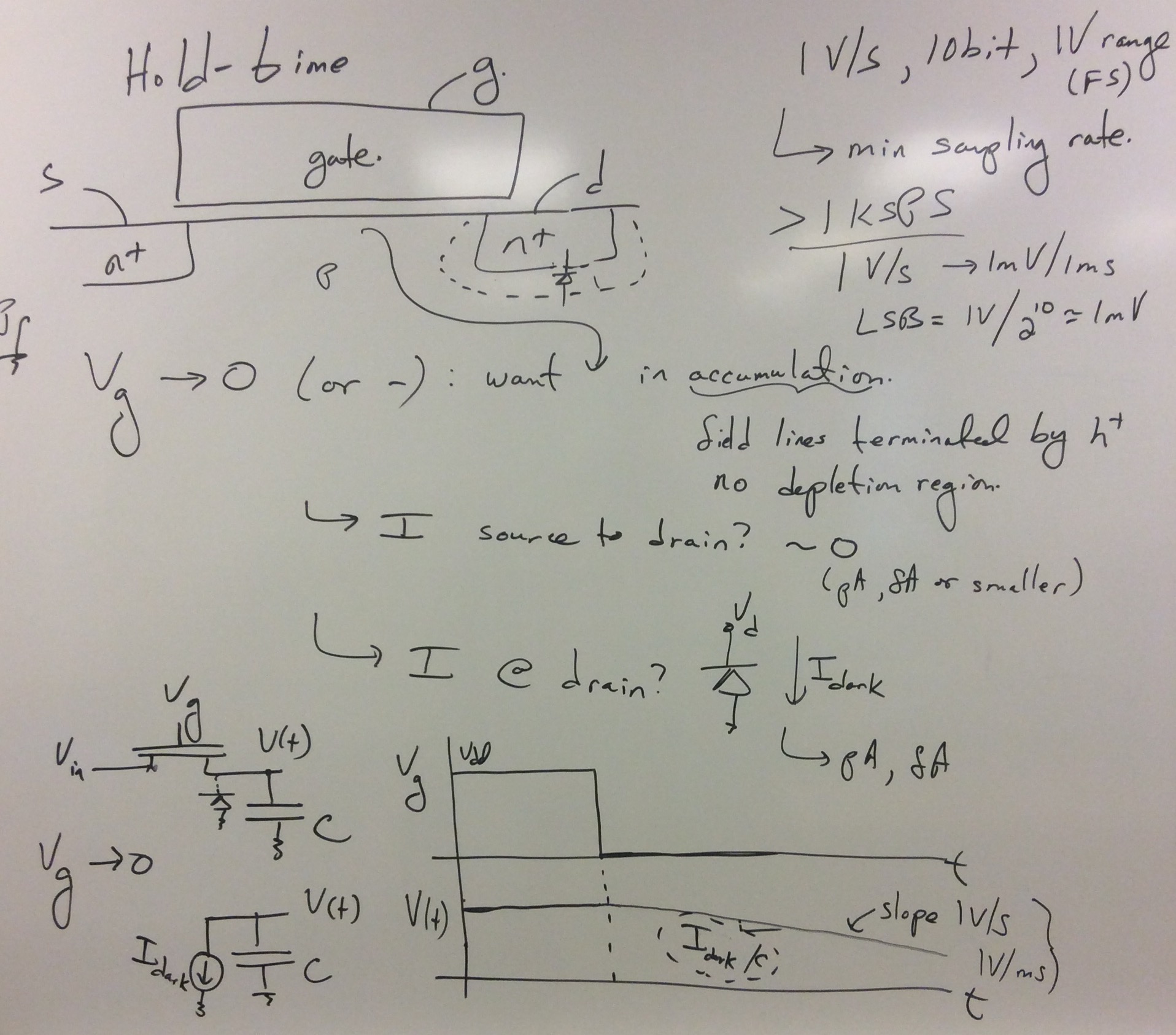
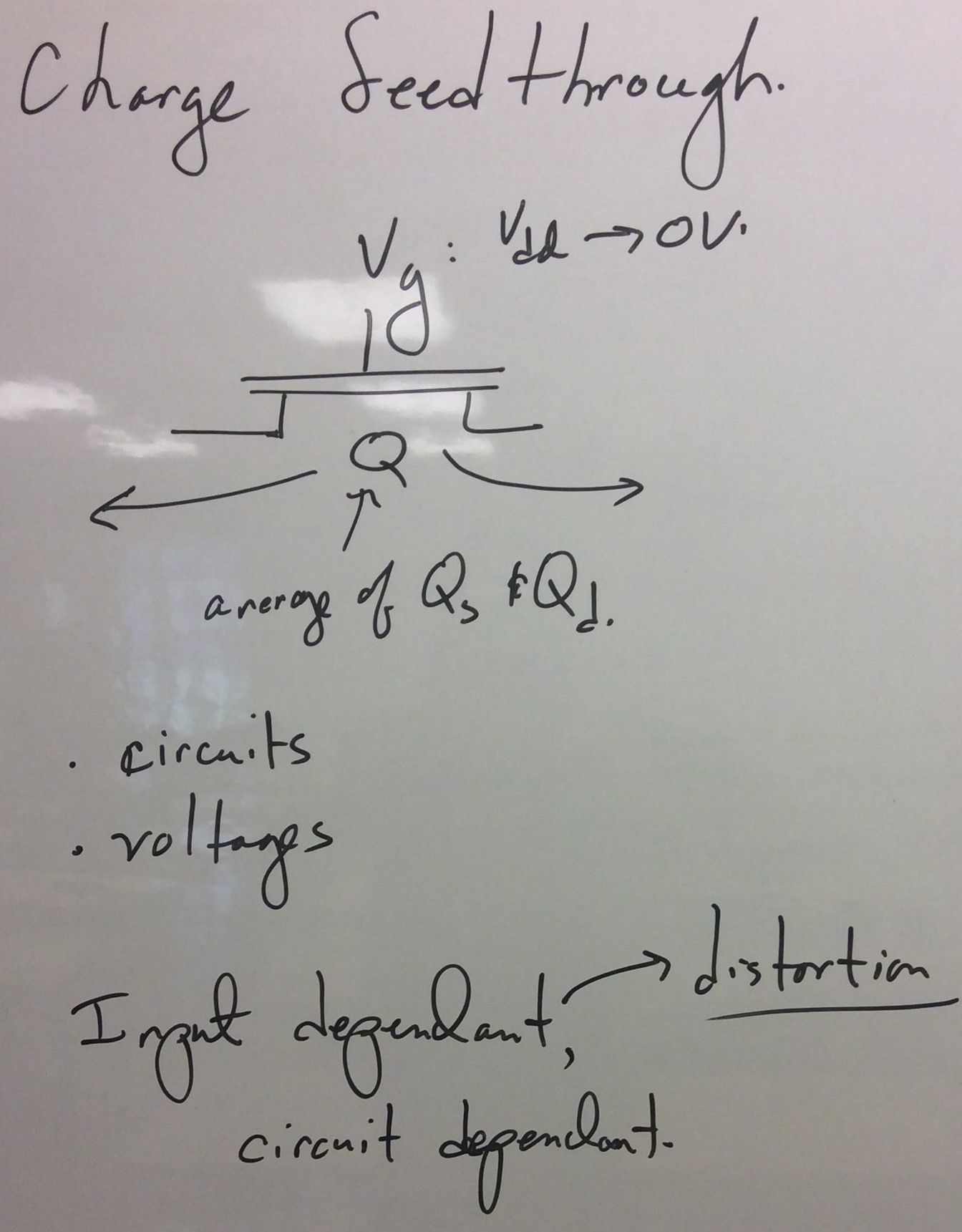
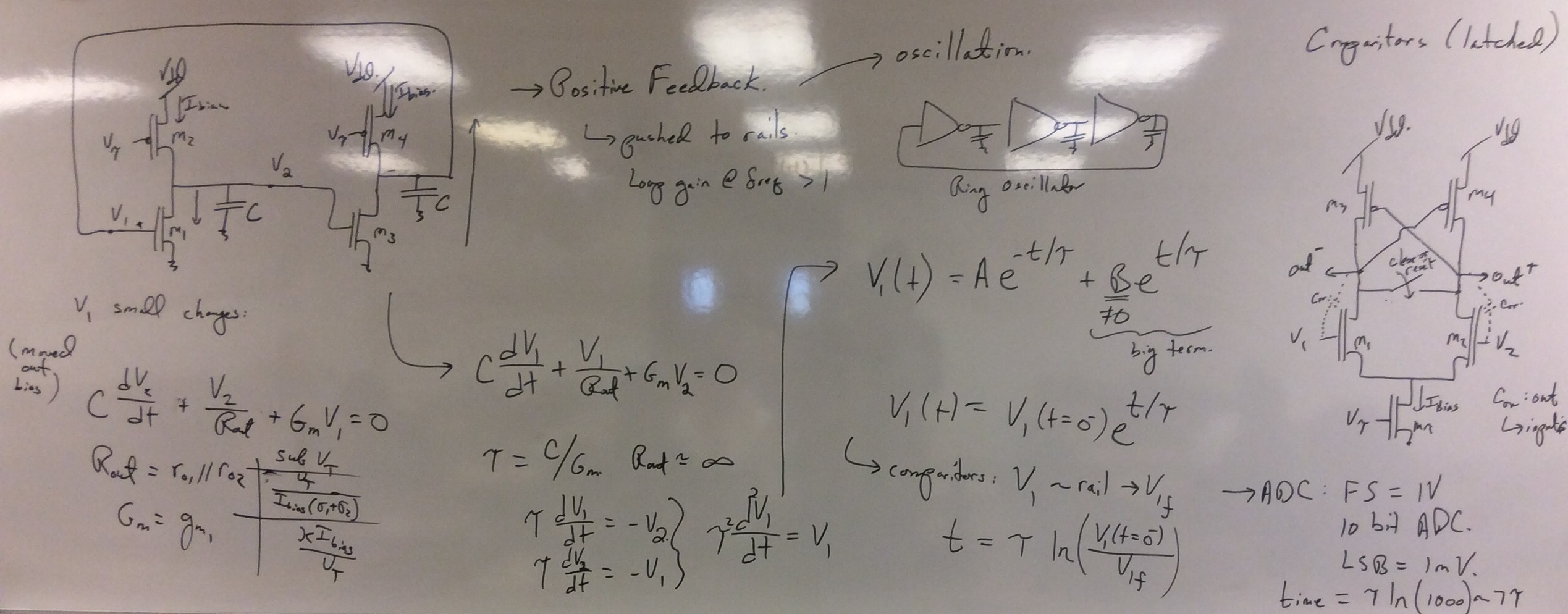
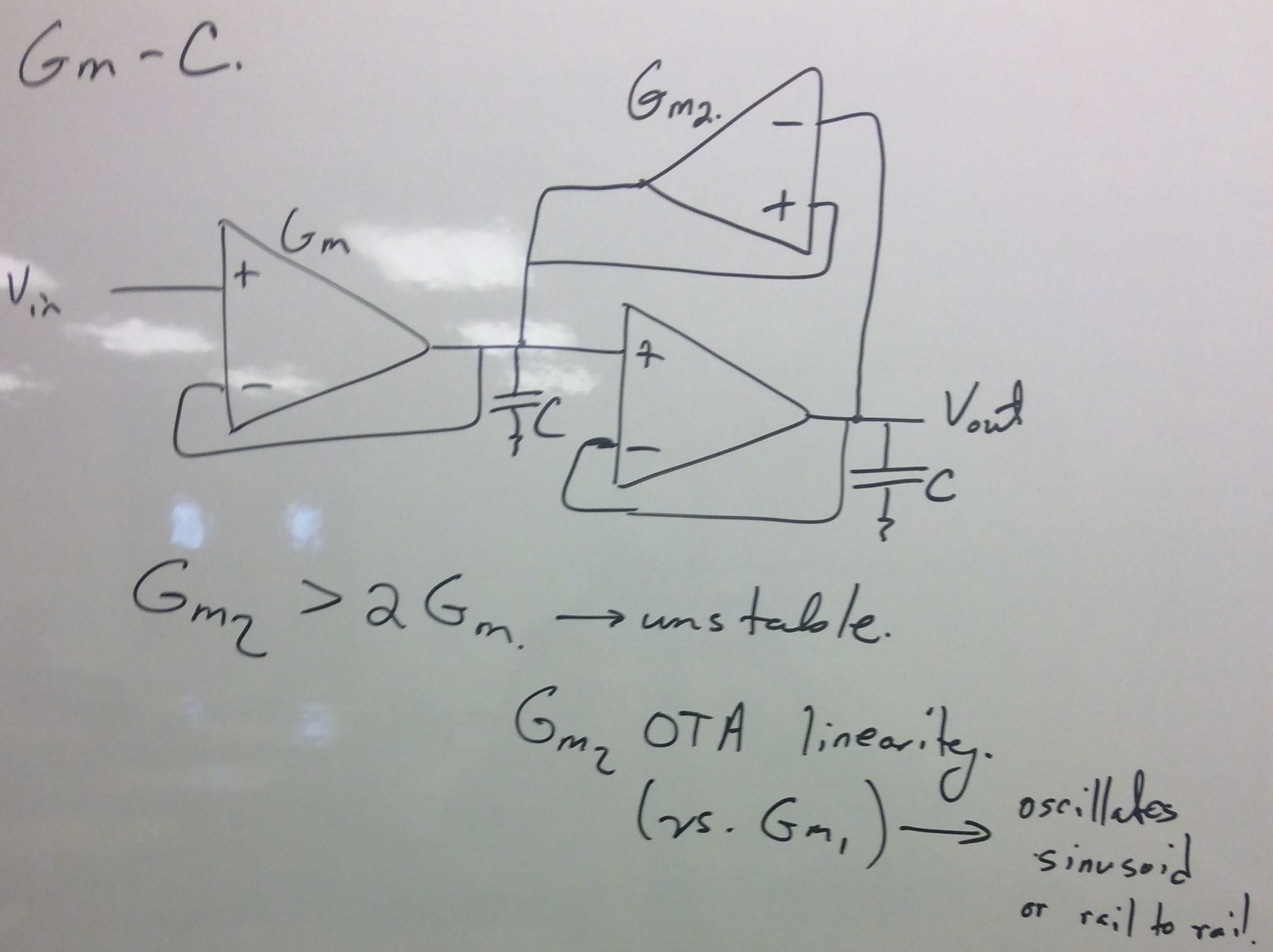
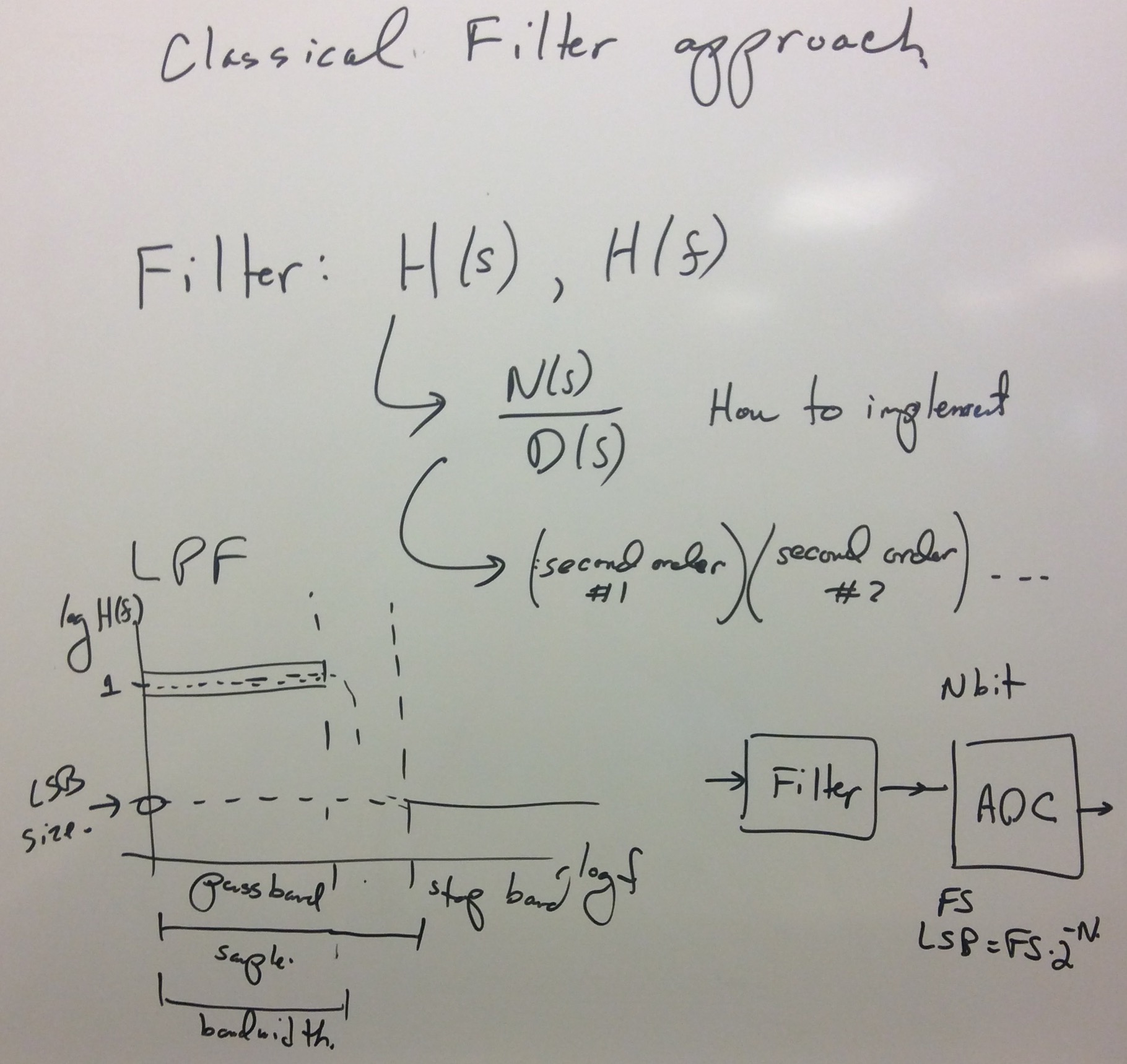
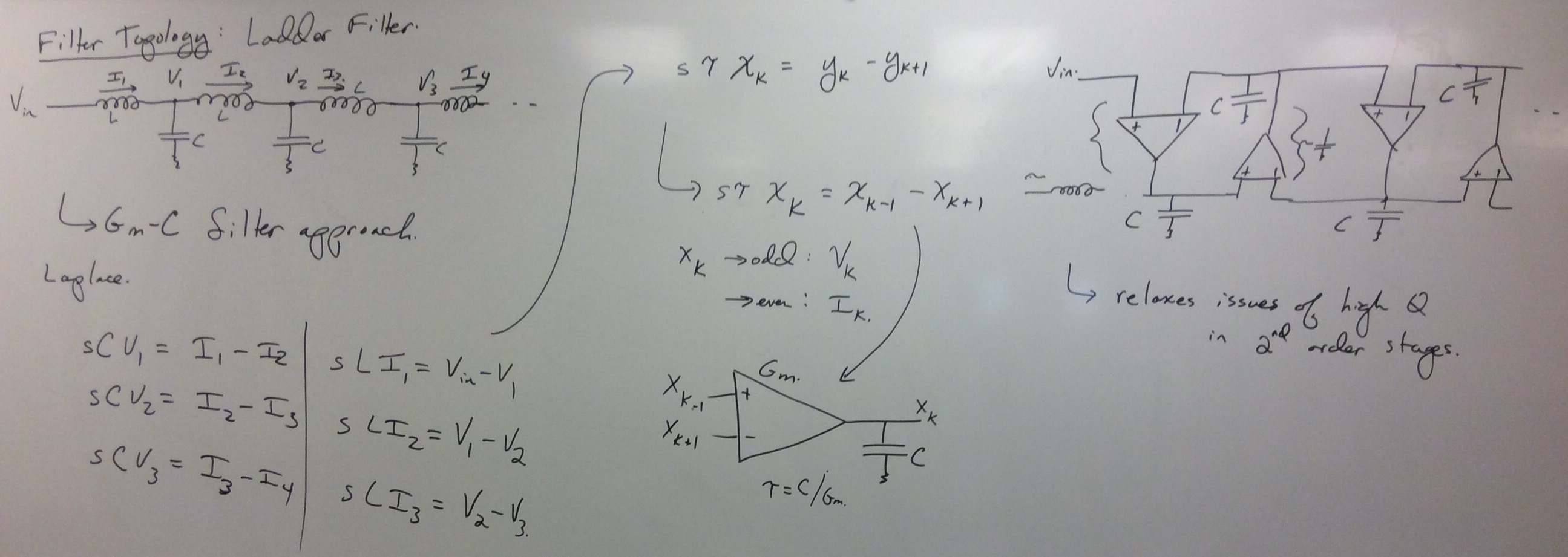
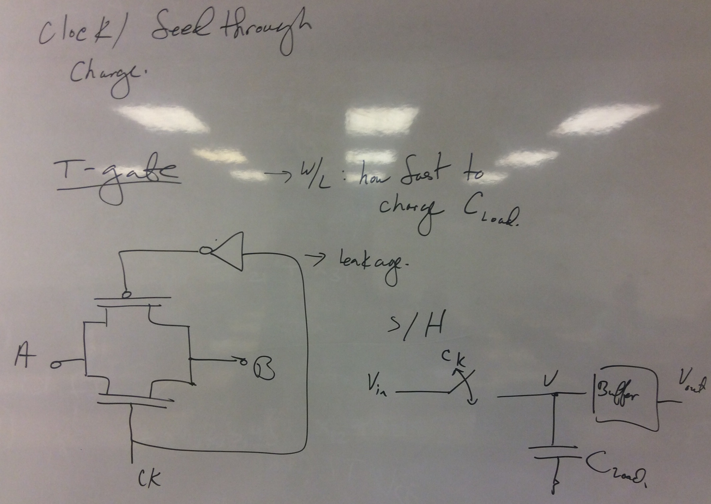
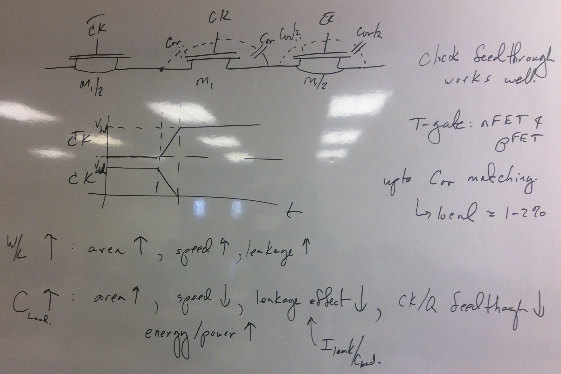
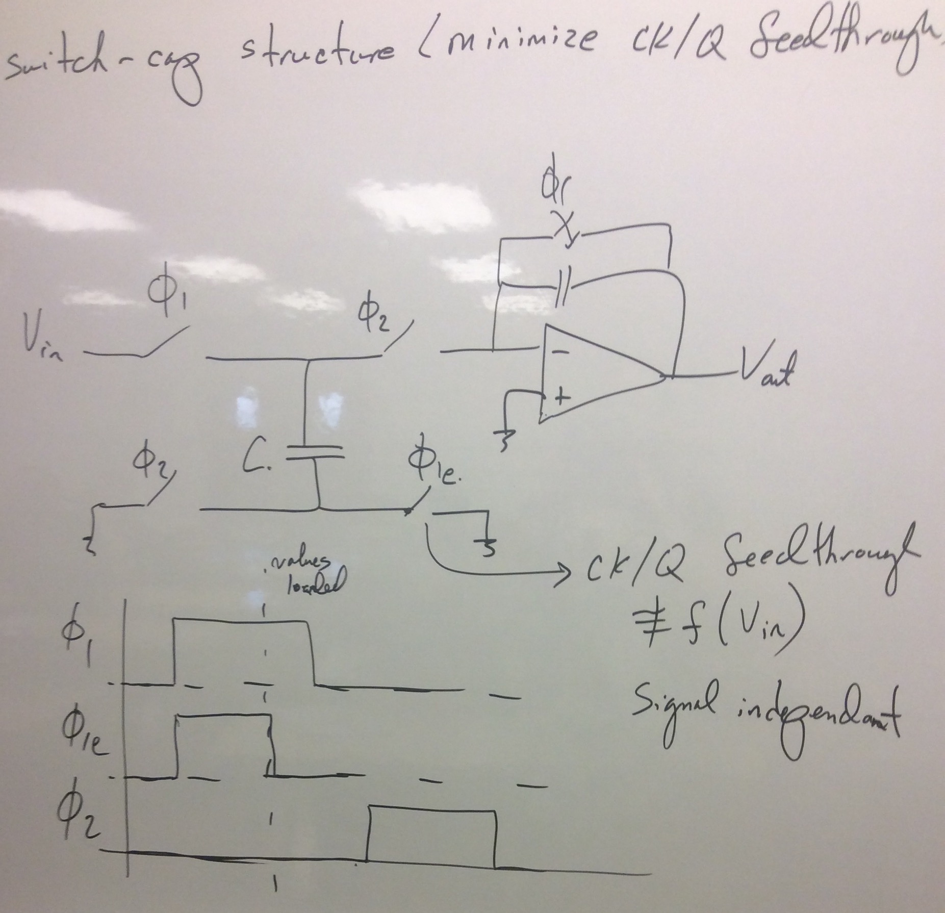
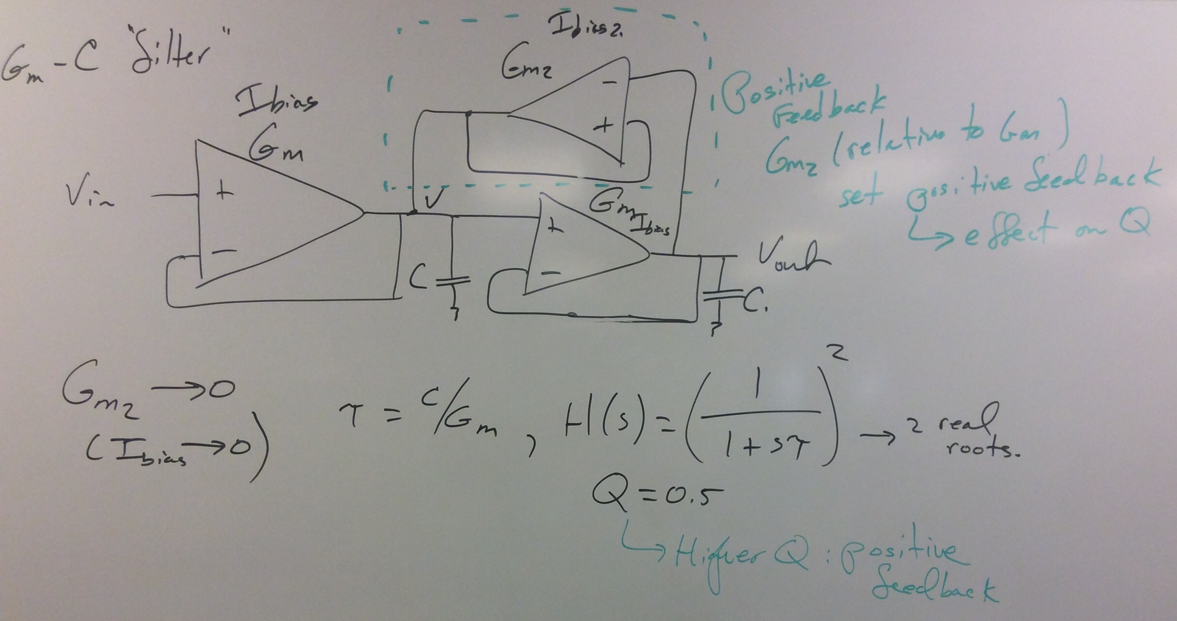
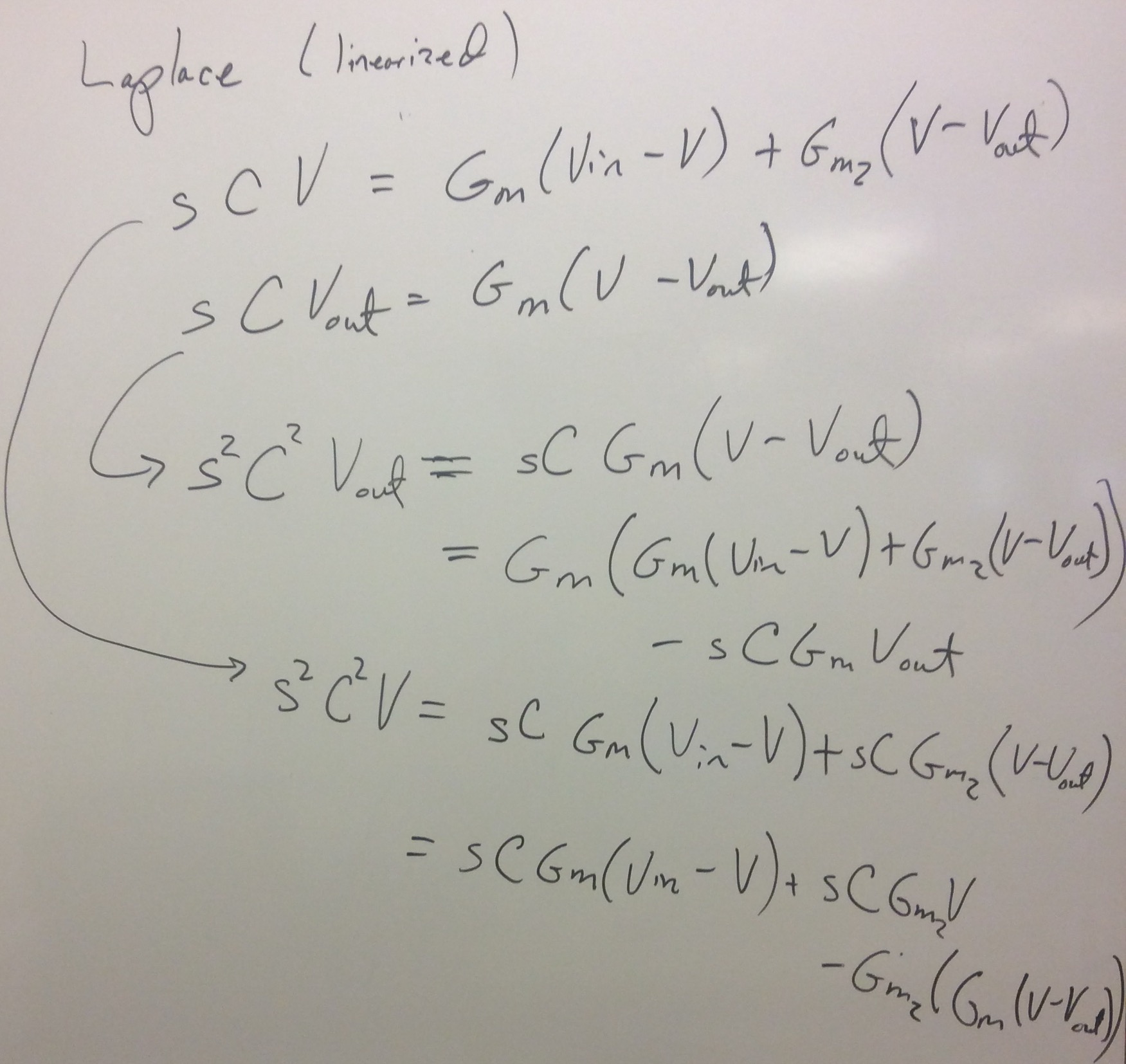
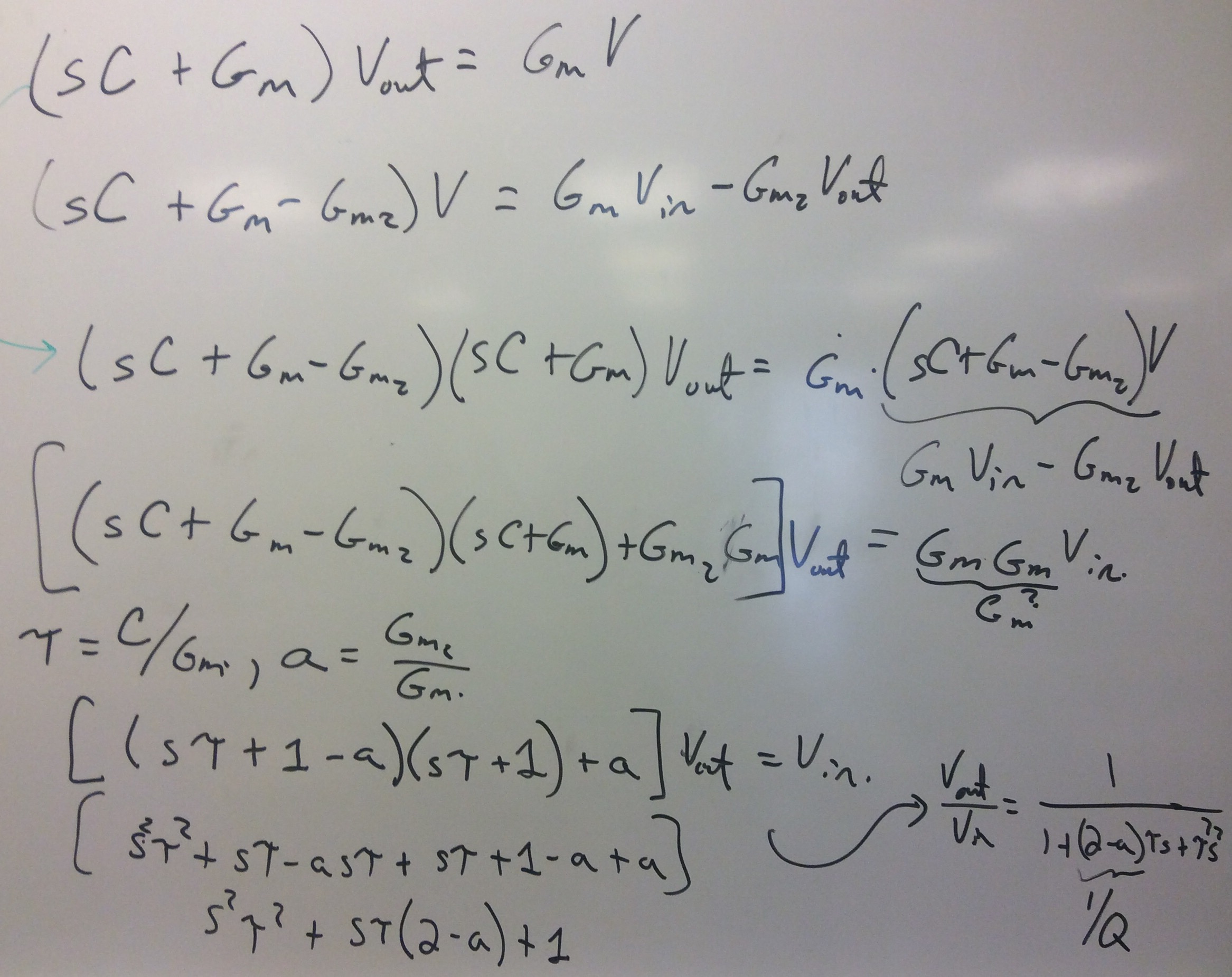
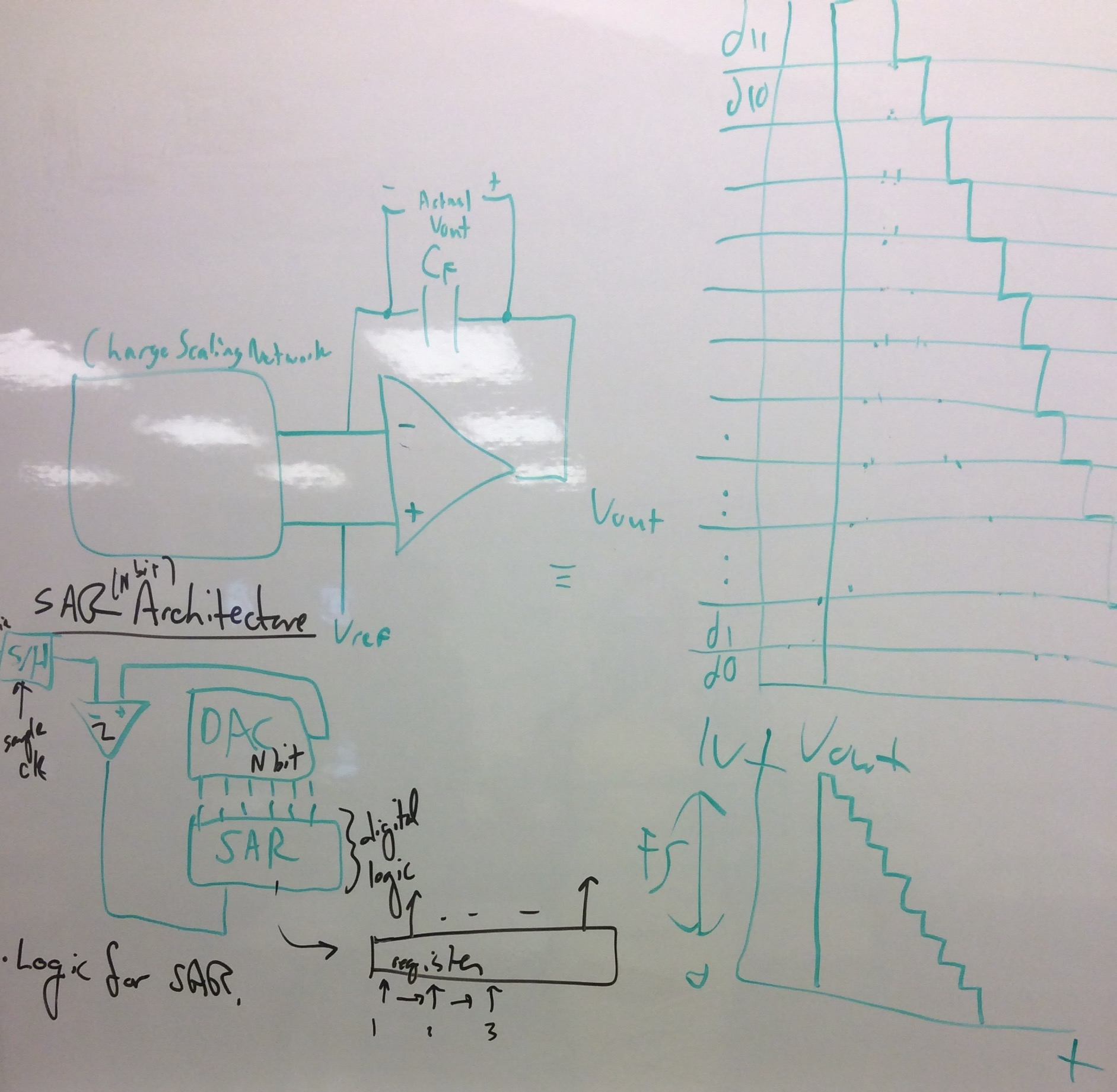
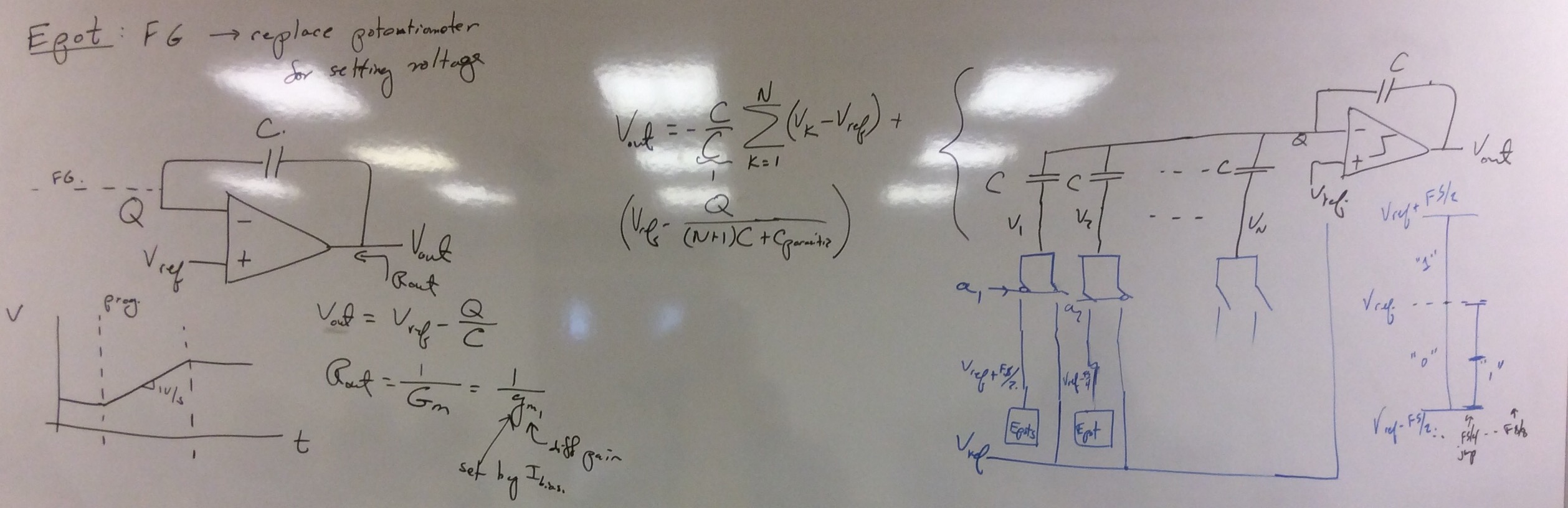
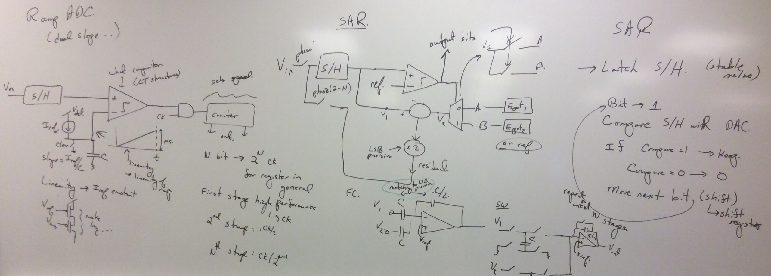
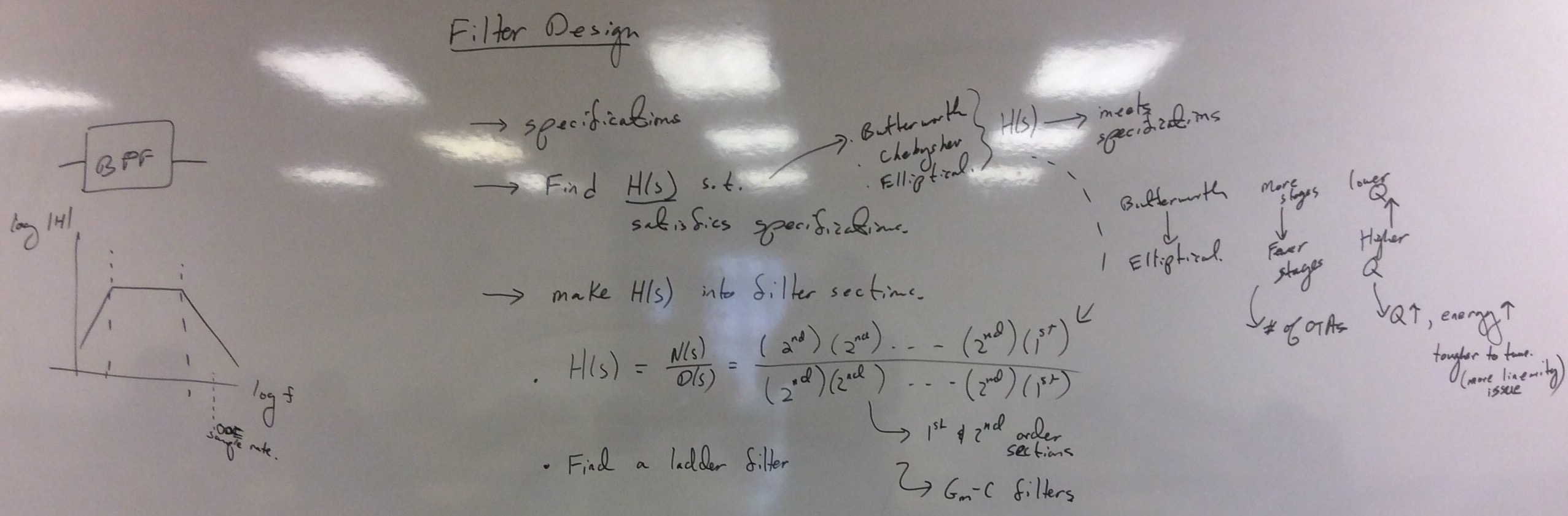
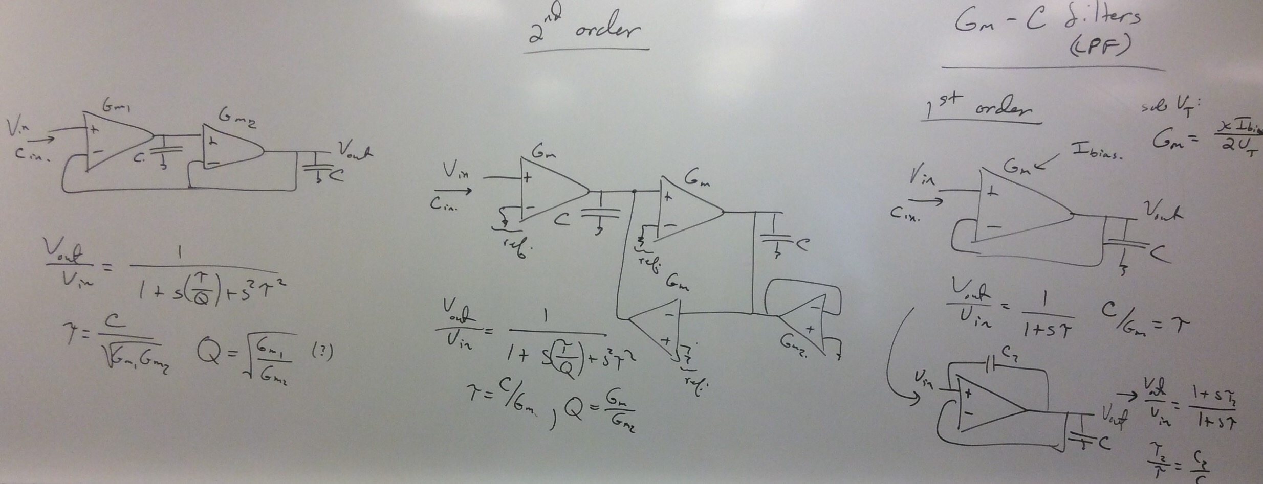
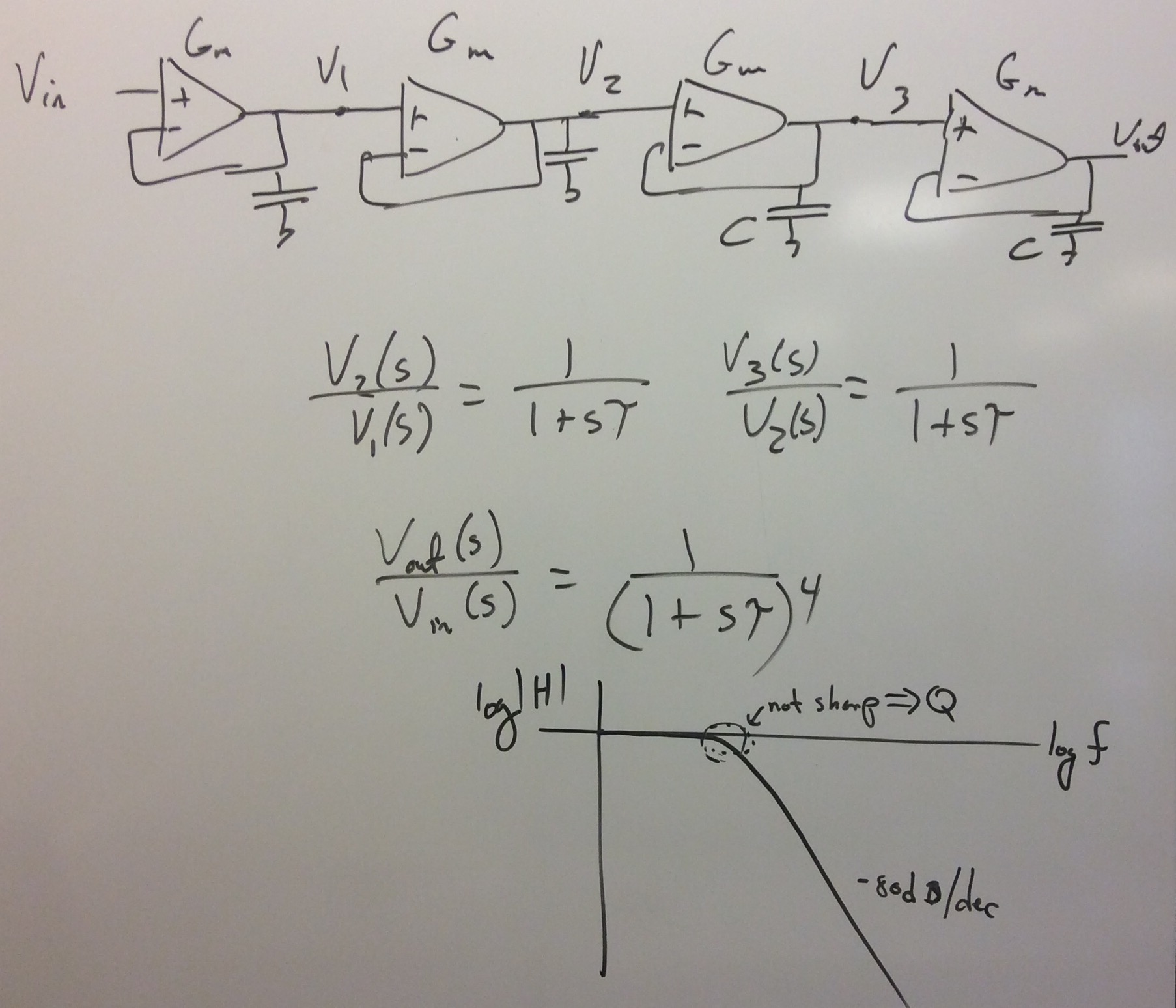
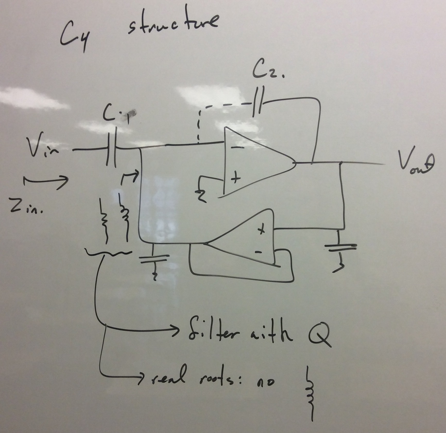
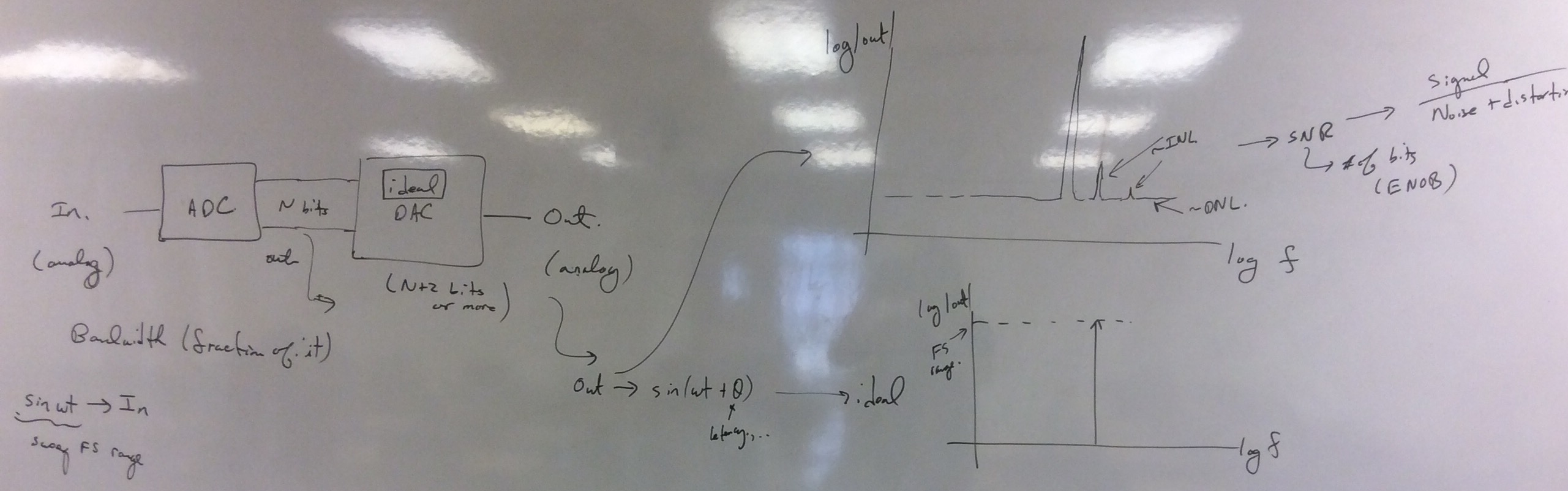
Previous Lecture Boards (2019)
Lecture Boards (2017)
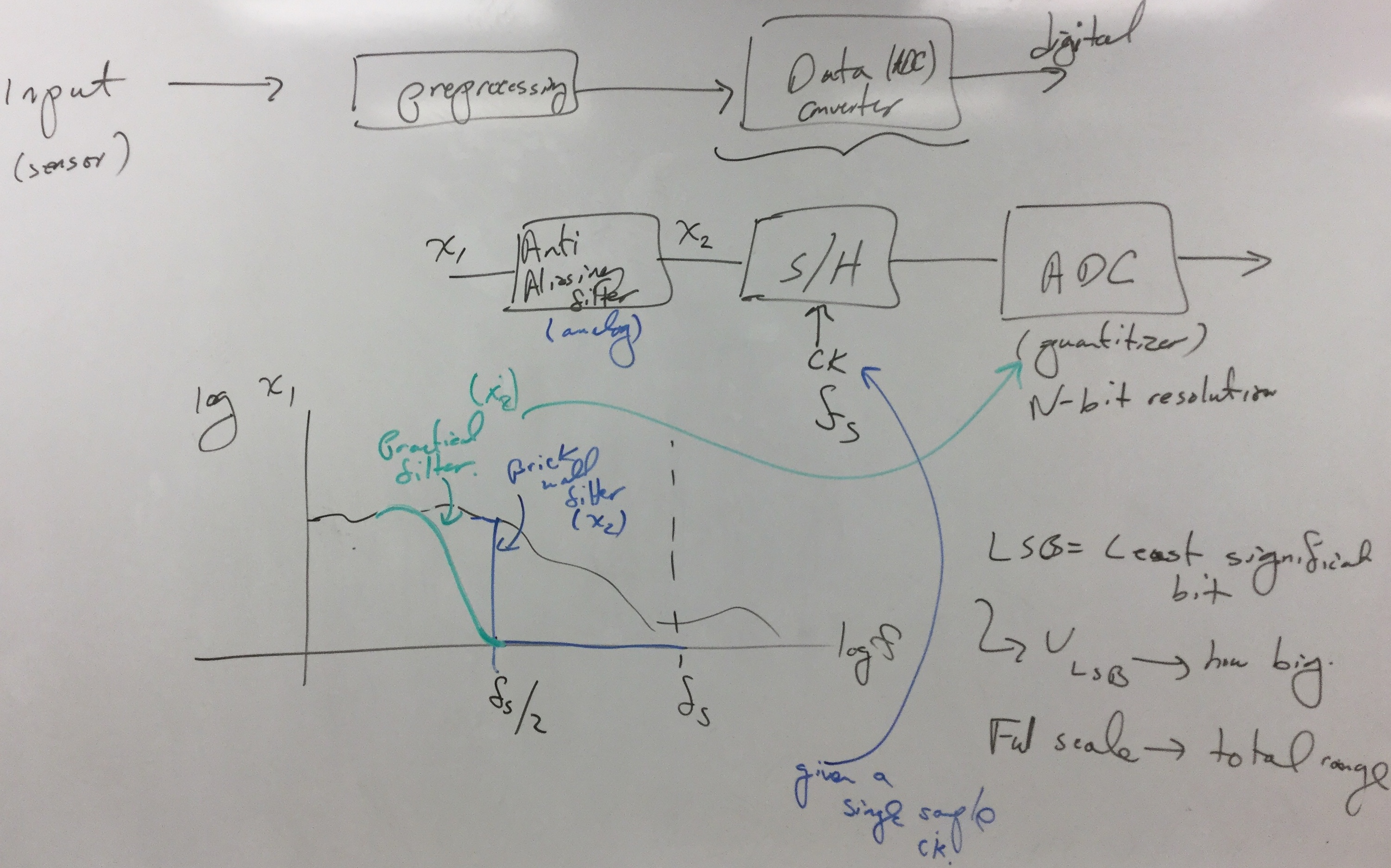
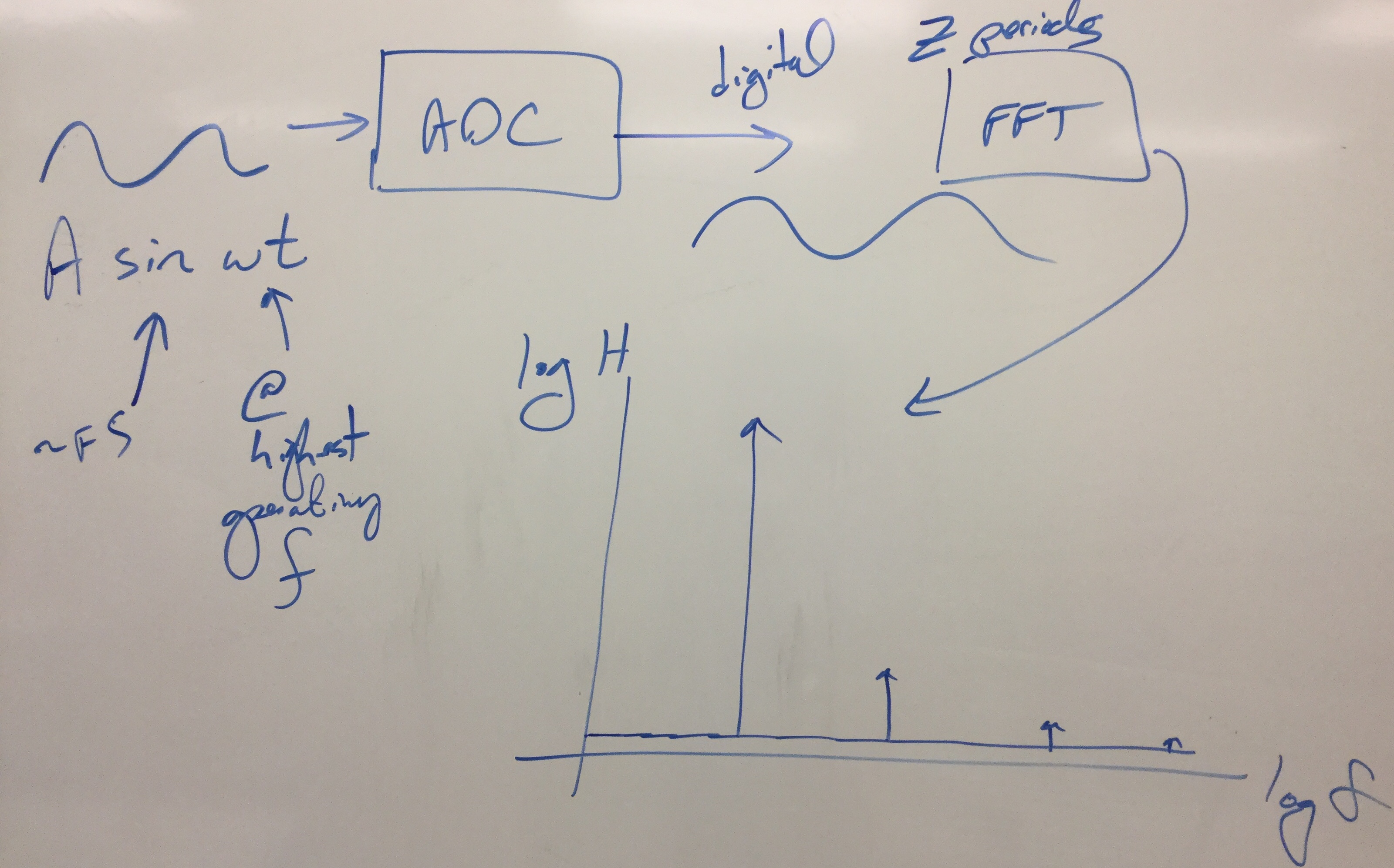
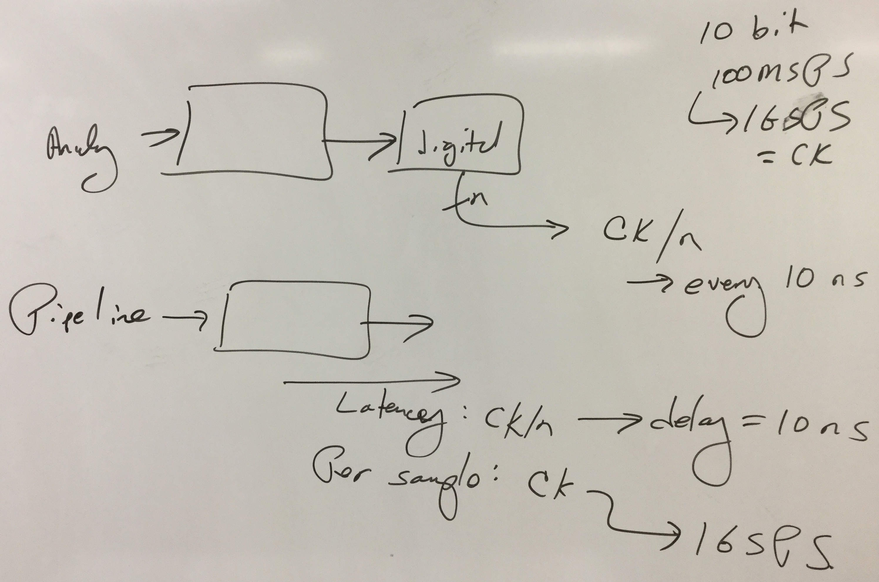
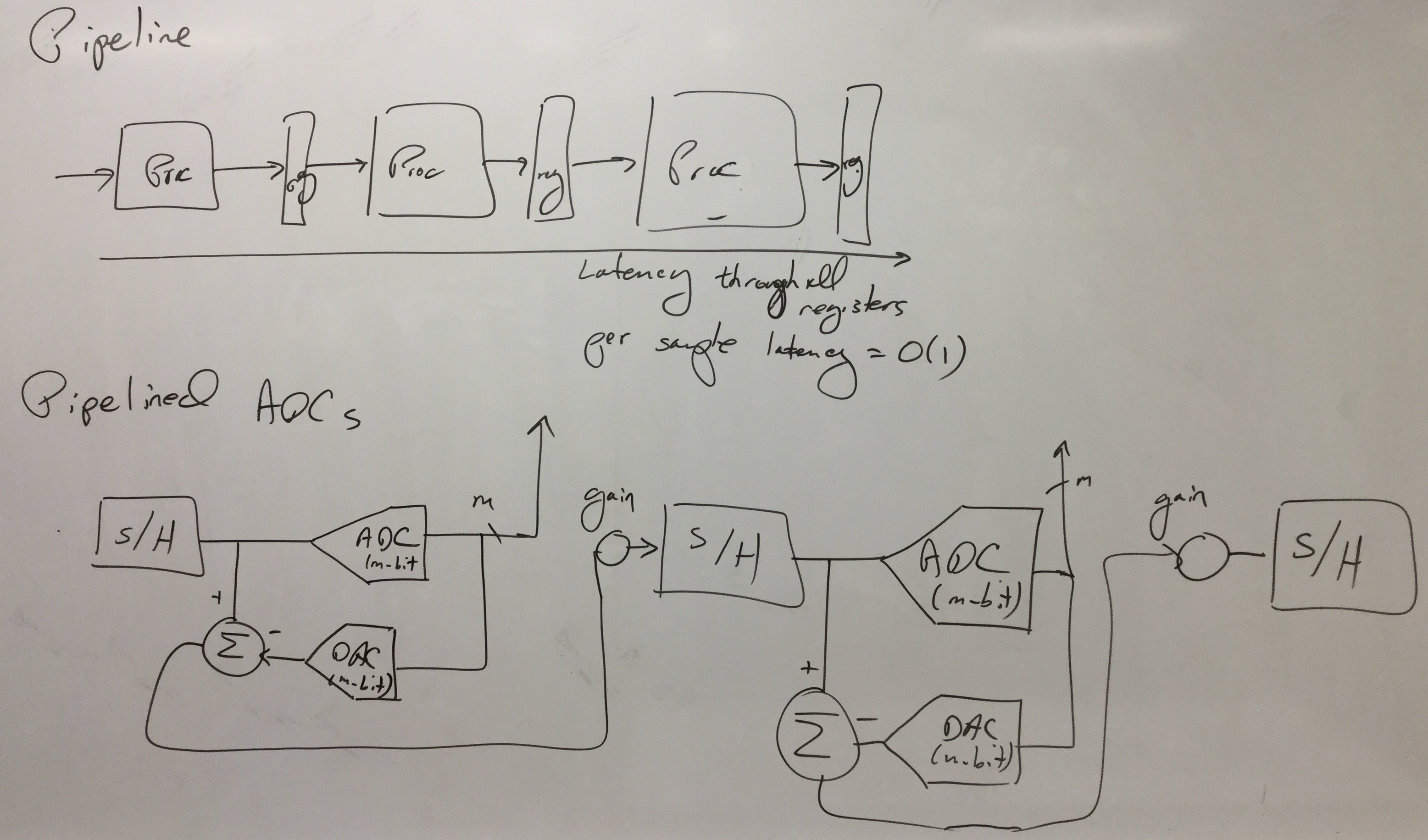
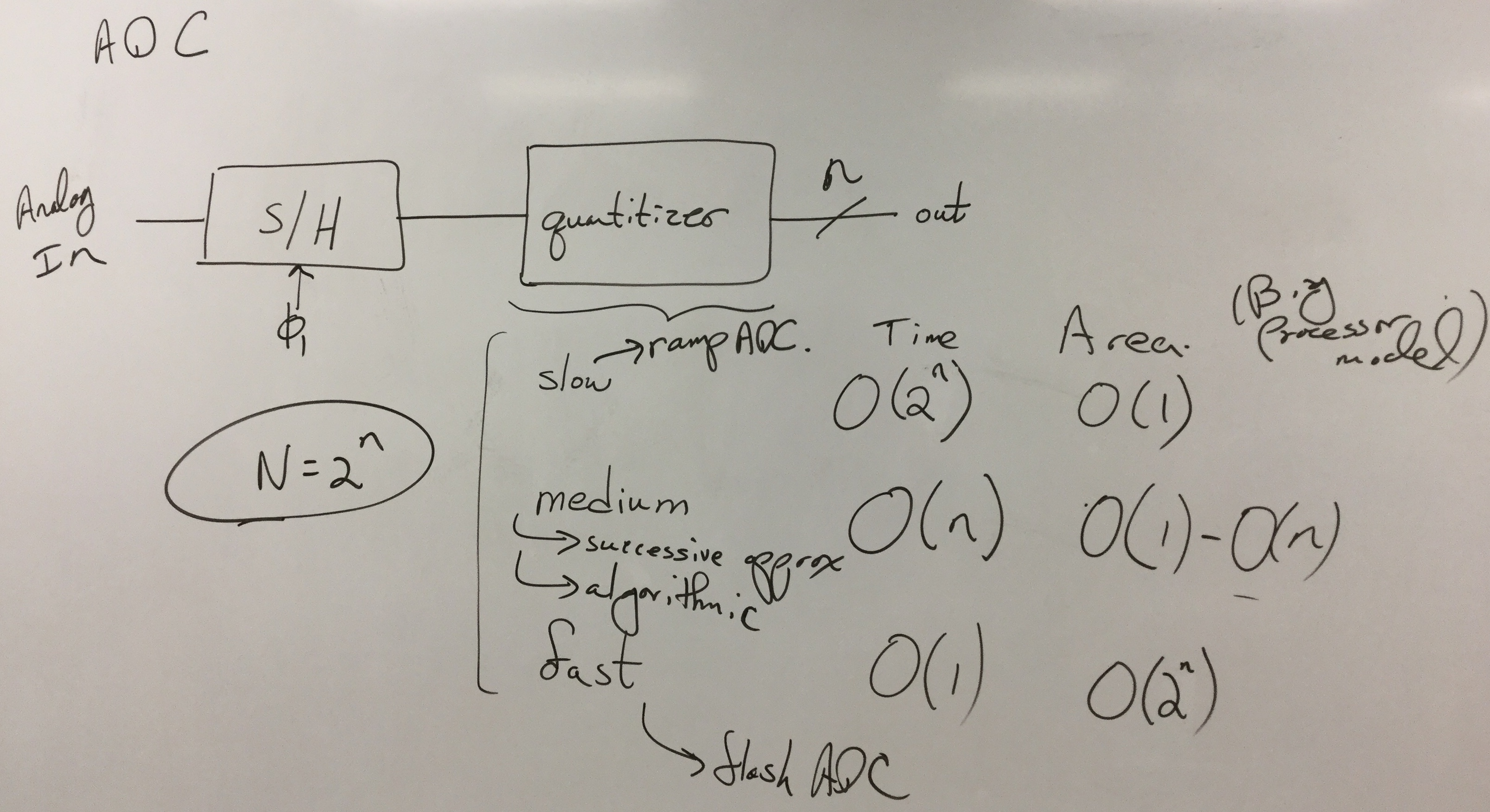
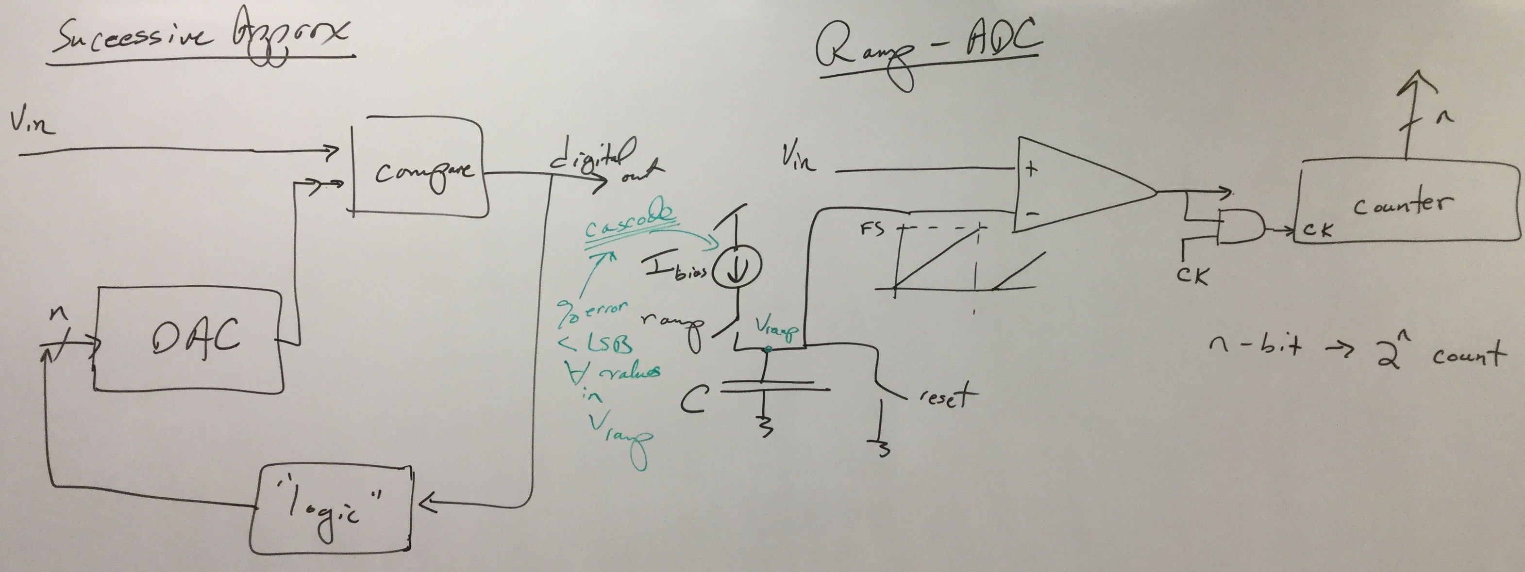
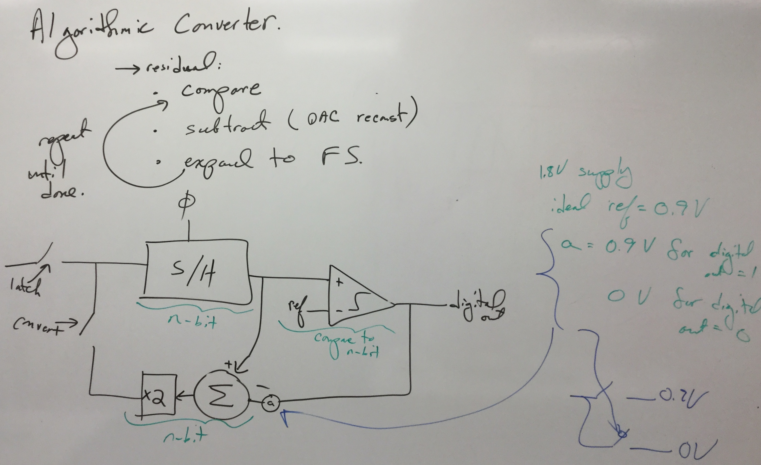
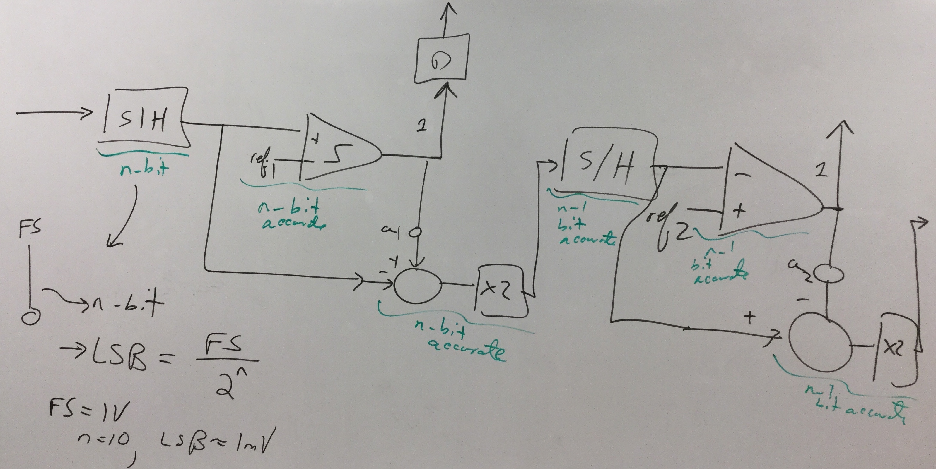
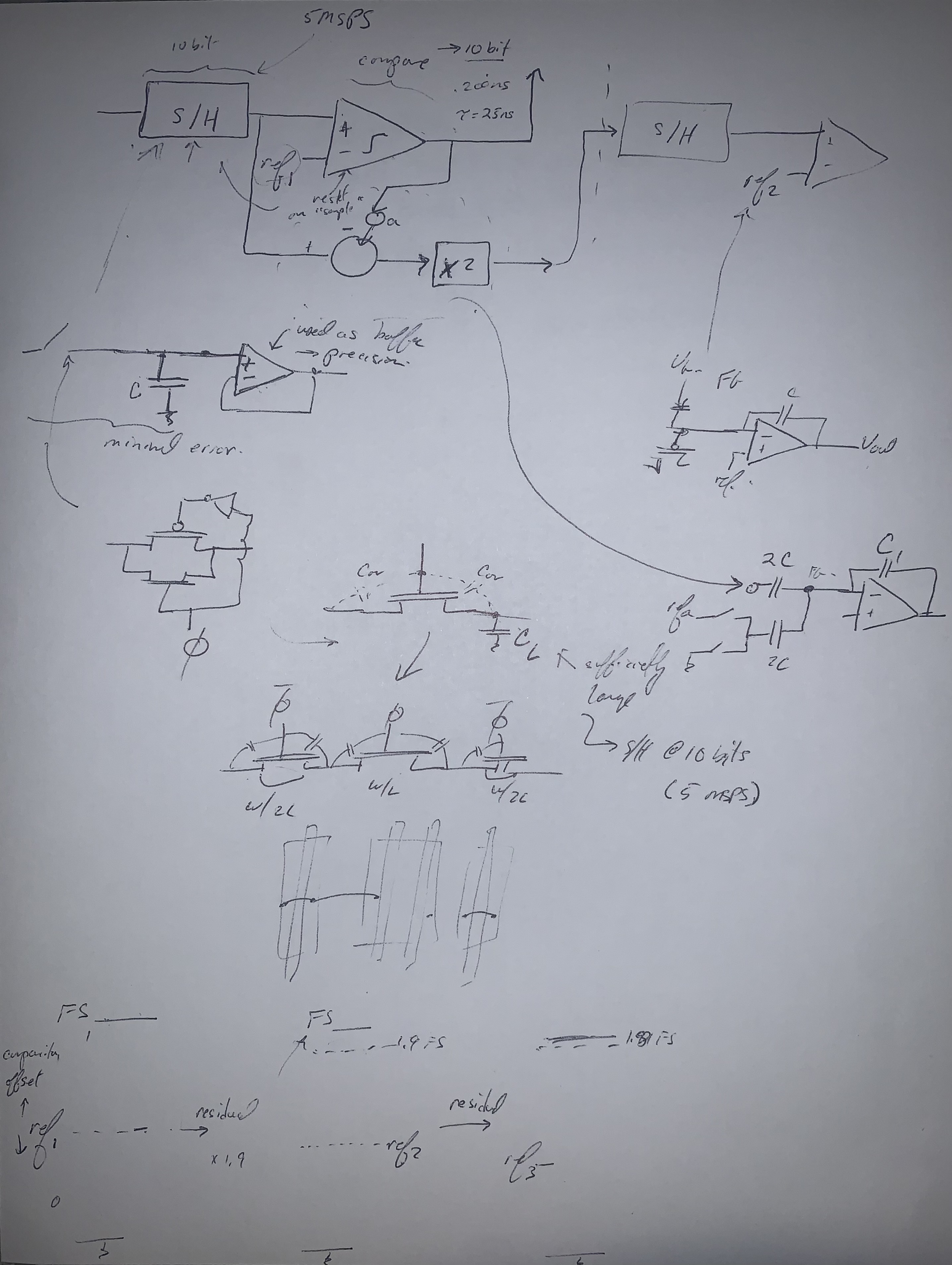
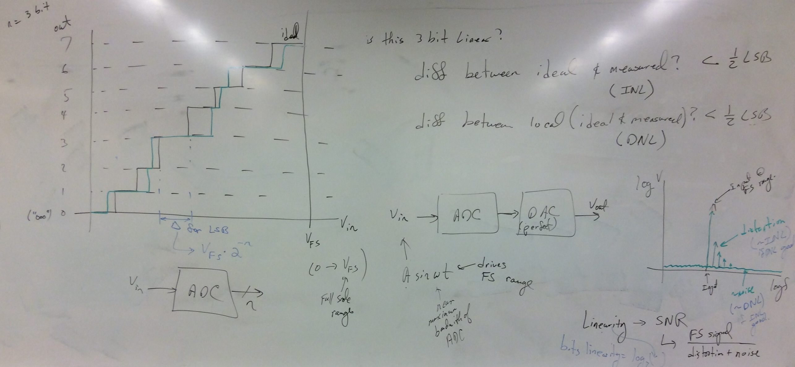
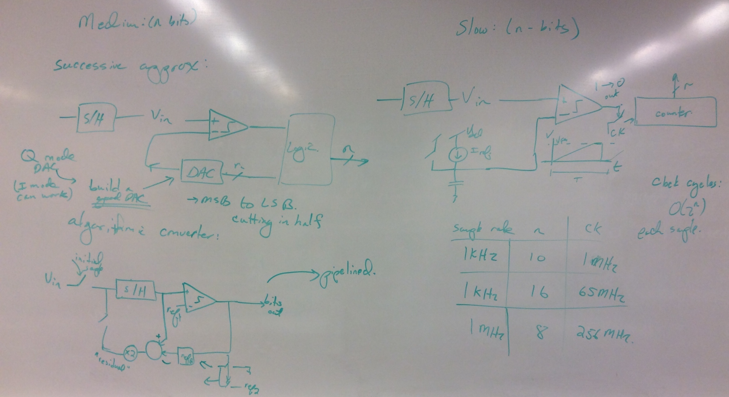
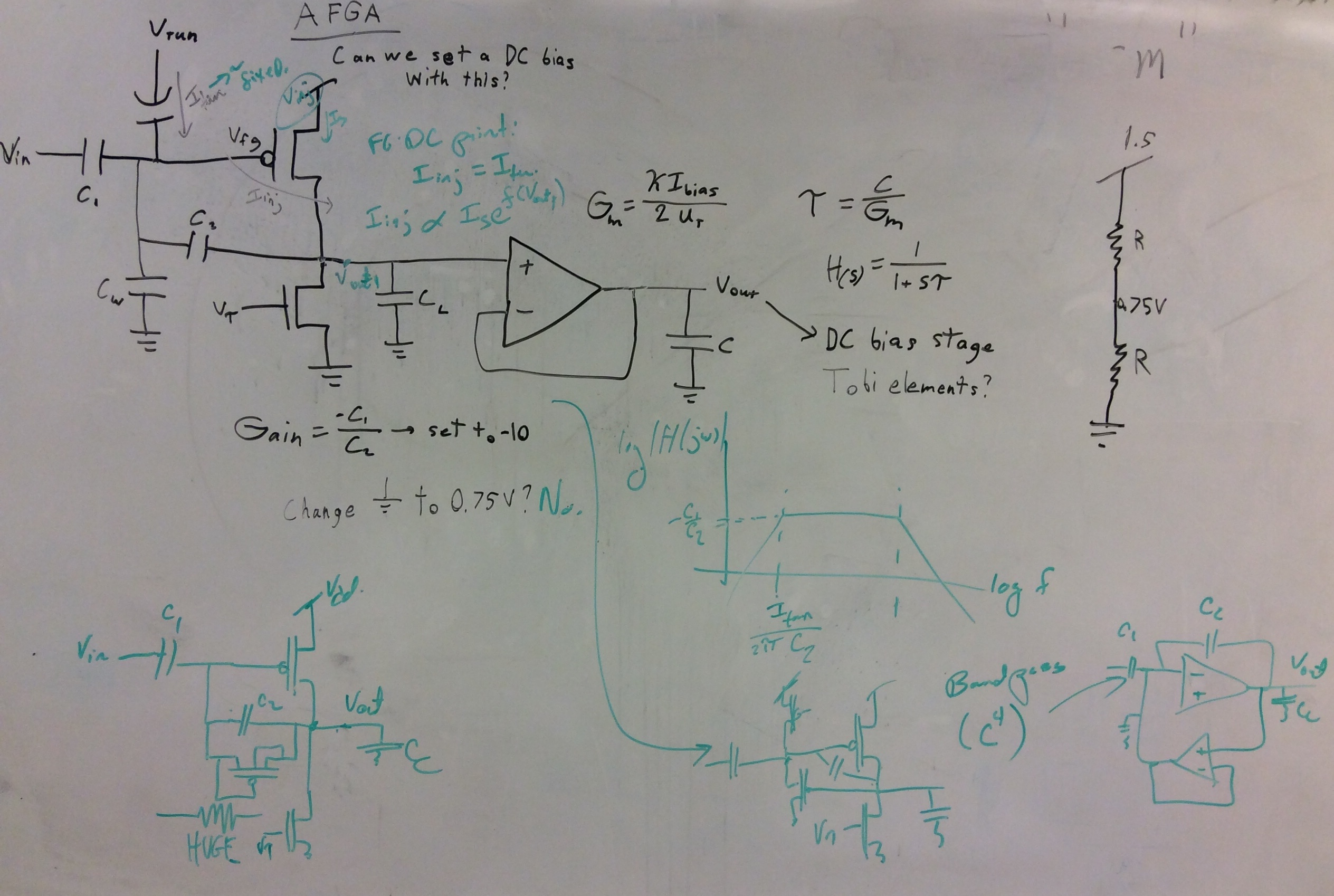
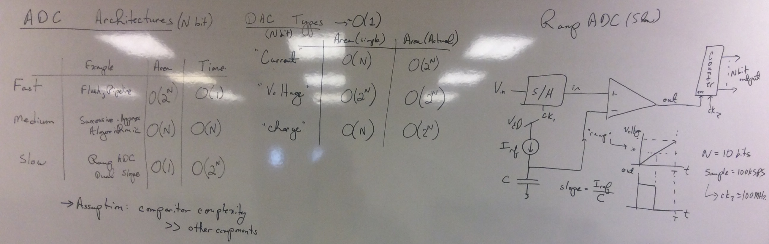
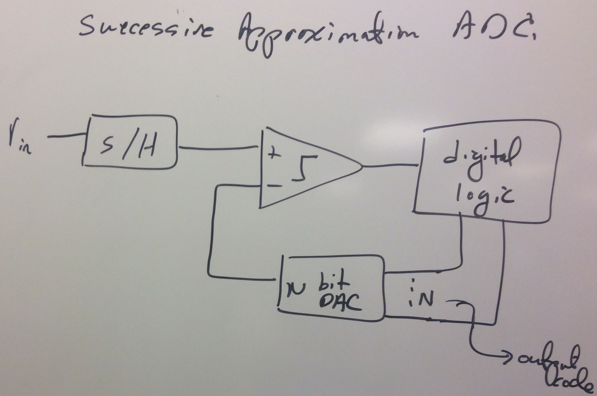
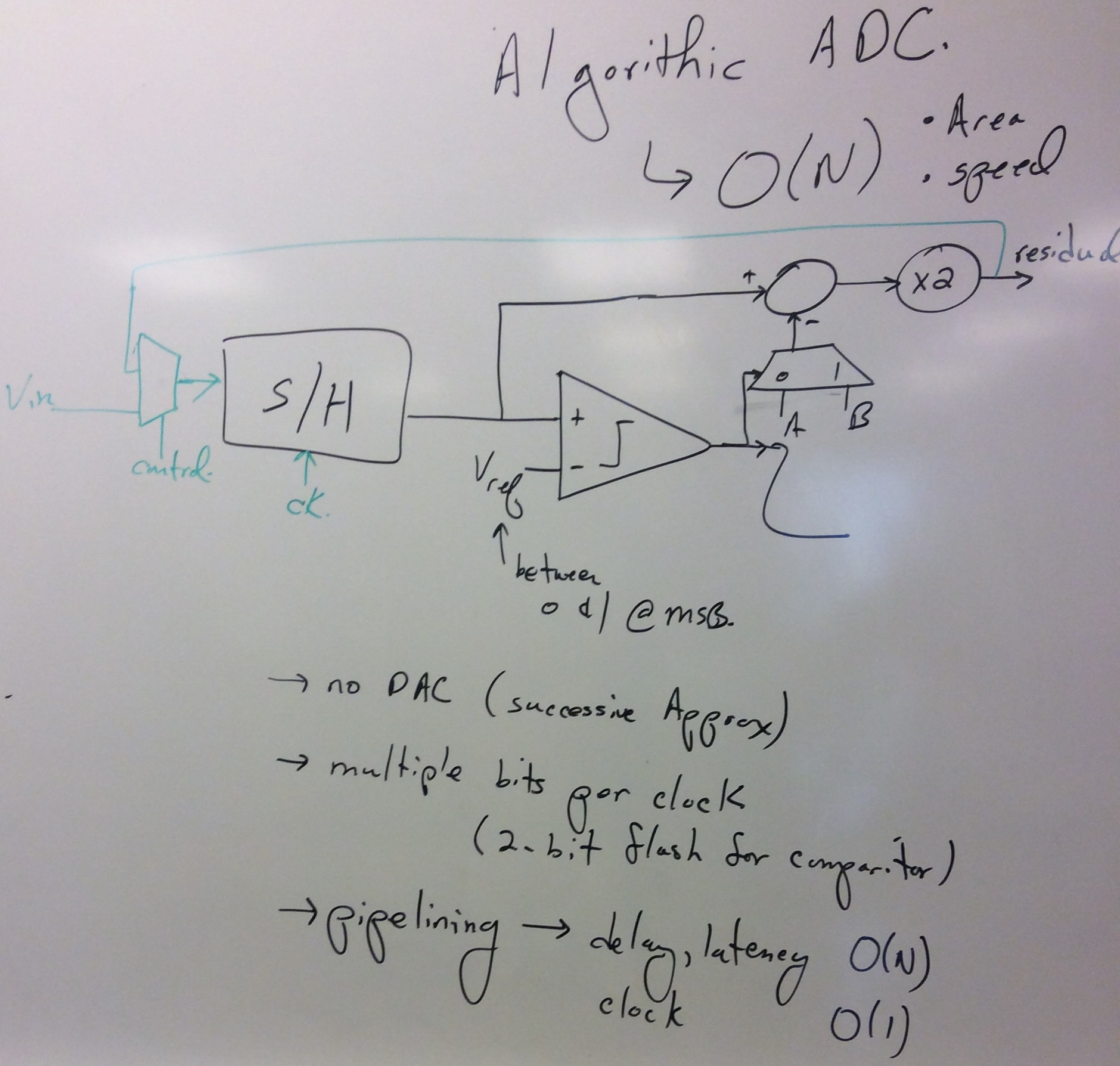
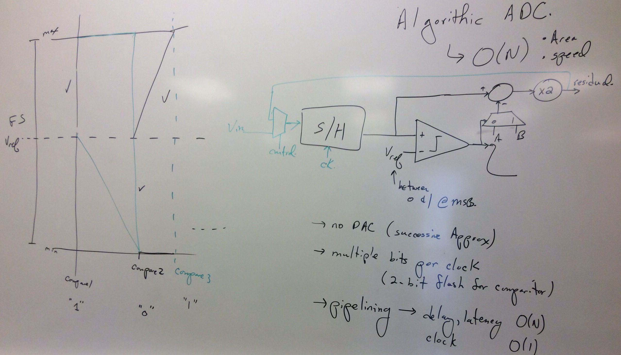
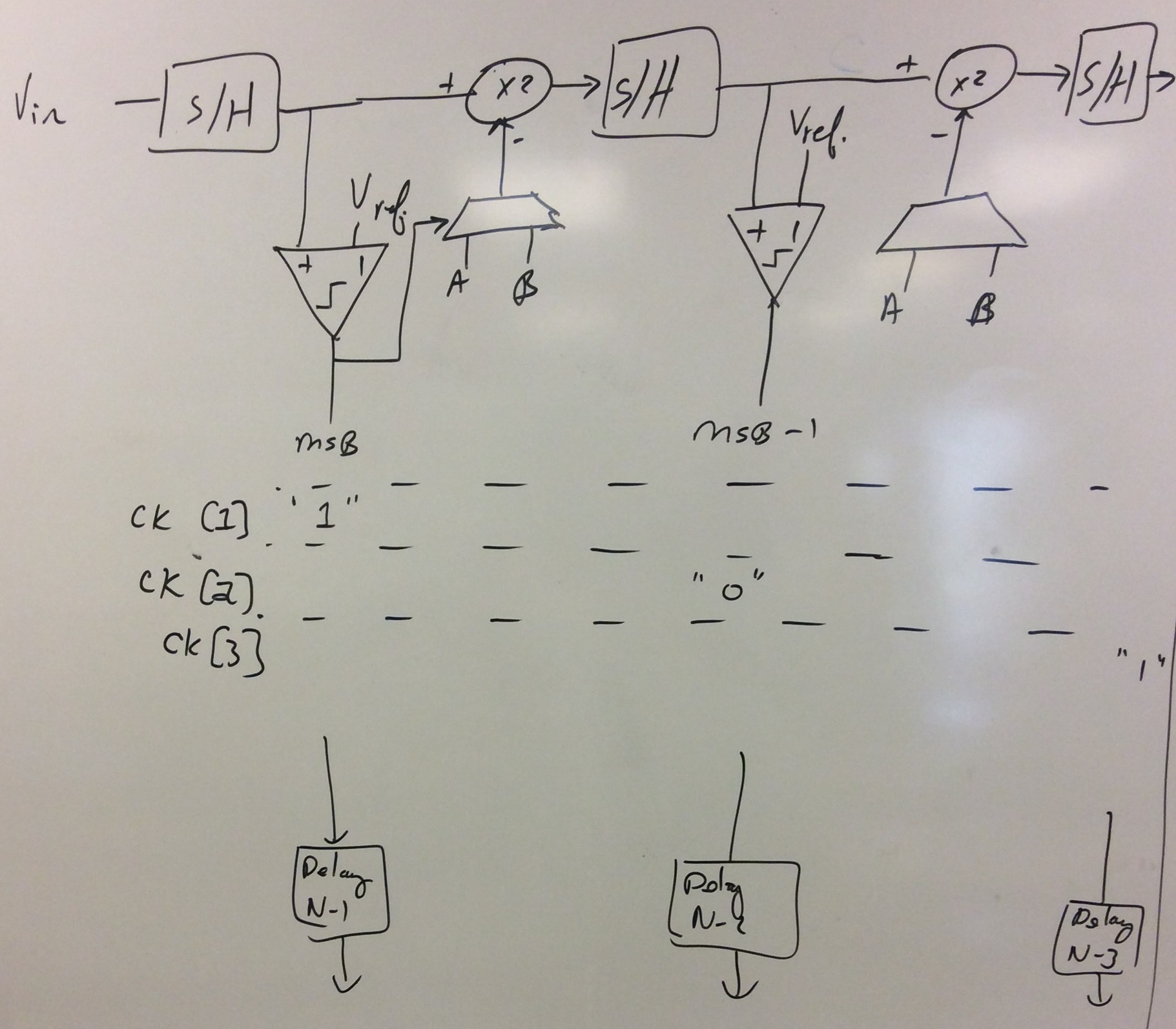
Analog System Design DescriptionAll blocks must be in pitch (6500nm). You may have multiple blocks and have higher level routing, but the final block still should be in pitch. Energy / Power must be minimized and is a major grading criteria. For all designs, optimizing power consumed as well as area are critical for both designs. The power supply for the IC will be 1.8V. The layout and post-layout simulation for this project is essential. Addressing matching between transistors is a critical discussion for these projects. As a reminder, FG techniques are allowed in your designs, assuming you have sufficient infrastructure to access the devices. For this project, Dec. 2 (Thursday) class session will be on-line, and each group will have a 7 minutes to describe their design and what they have done to this point. One might expect 5-7 slides. The purpose of this discussion is an opportunity for everyone in the class to learn about the other designs, as well as to get feedback on the design to improve the design before submission. System Design 1: An Algorithmic ADCThis system design will be to make a 10bit capable Algorithmic ADC converter. Figure 1 shows the basic block diagram for an Algorithmic ADC. You can either build a single stage or a pipelined stage; no digital post-correction should be required or used for these designs. The core Algorithmic ADC block, whether pipelned or not, should be a separate block. You want a 1.2V full-scale range in the 1.8V power supply range. The sampling rate is given specifically to each group.
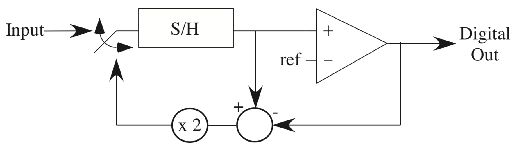
Fig. 1: Block Diagram for an Algorithmic Analog-to-Digital Converter Topology.
Layout items to submit :
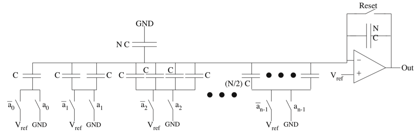
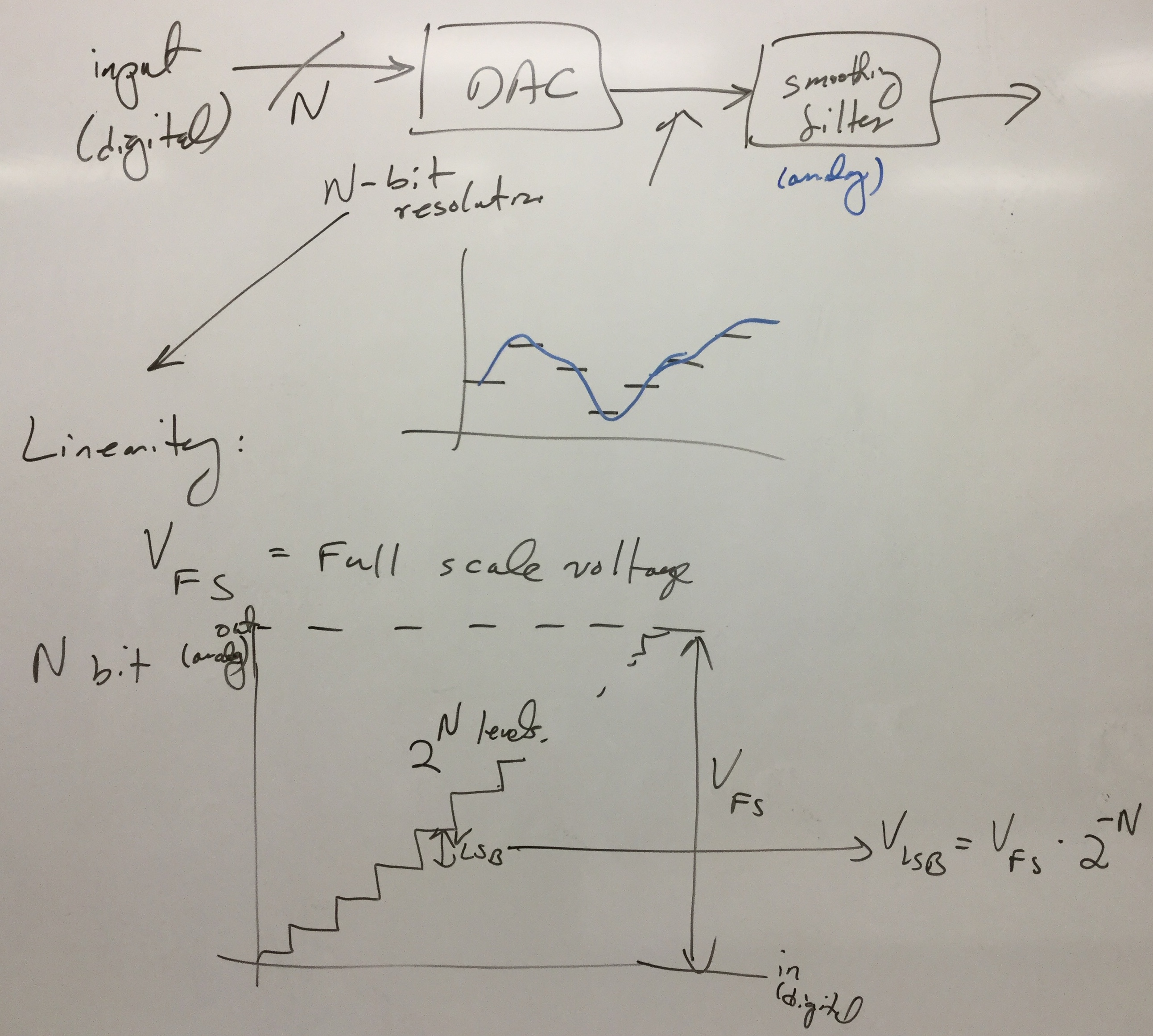
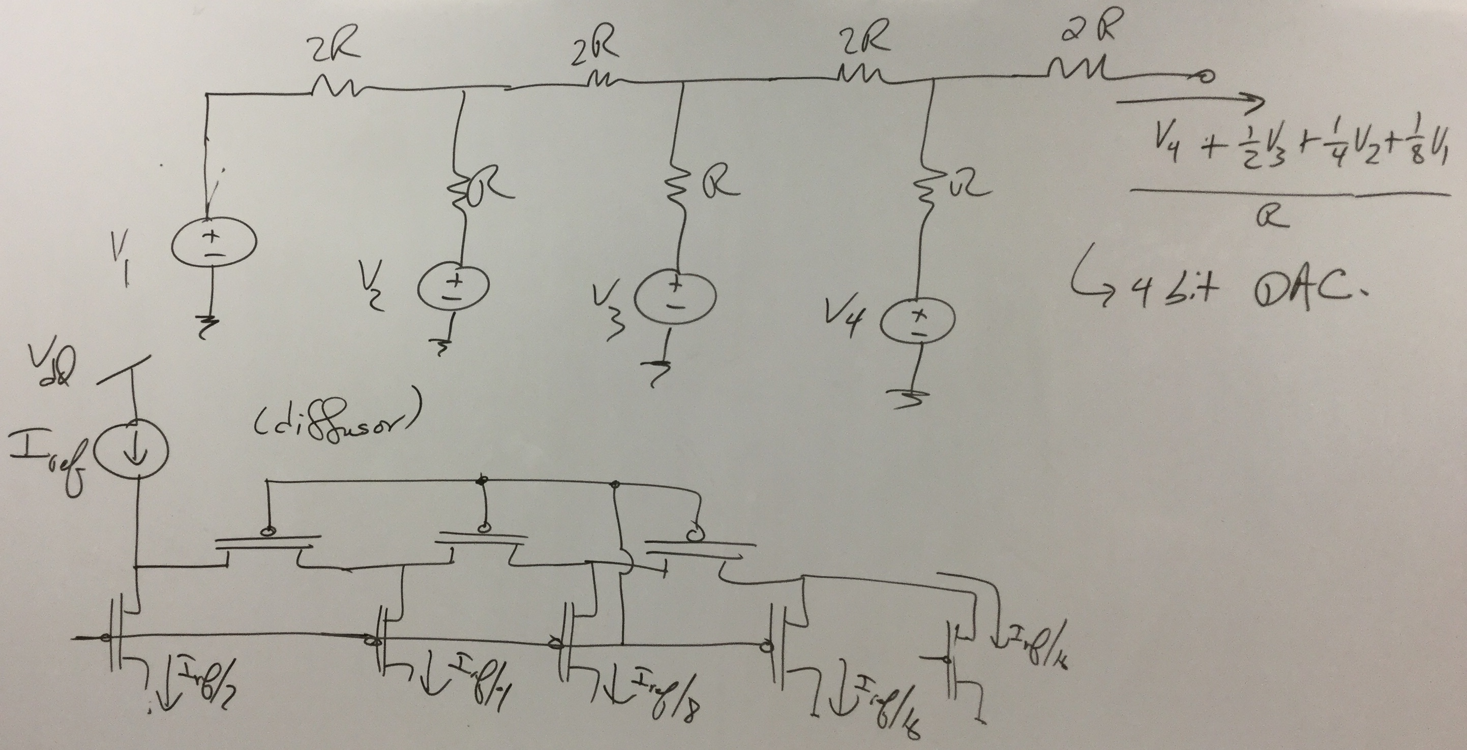
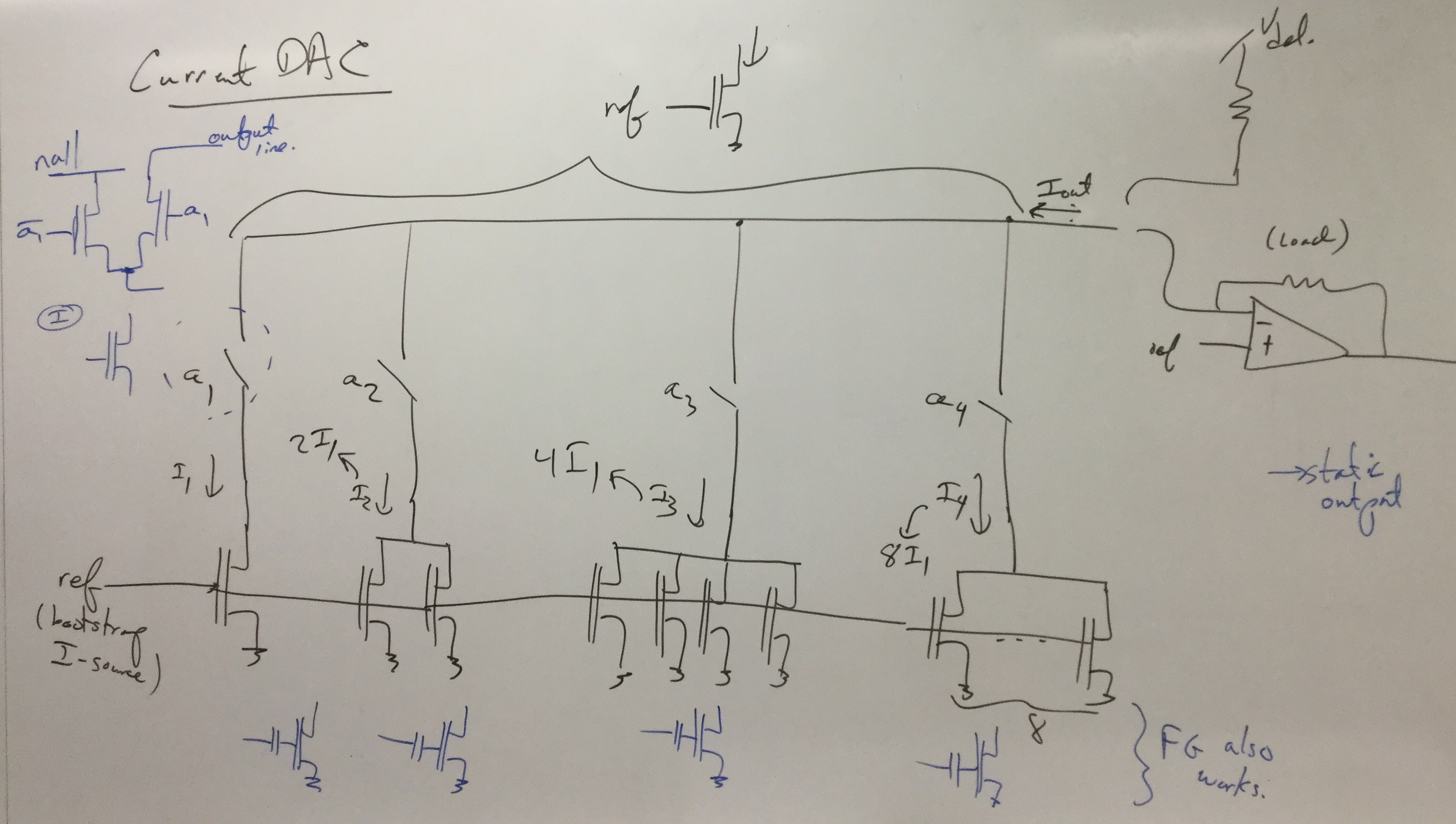
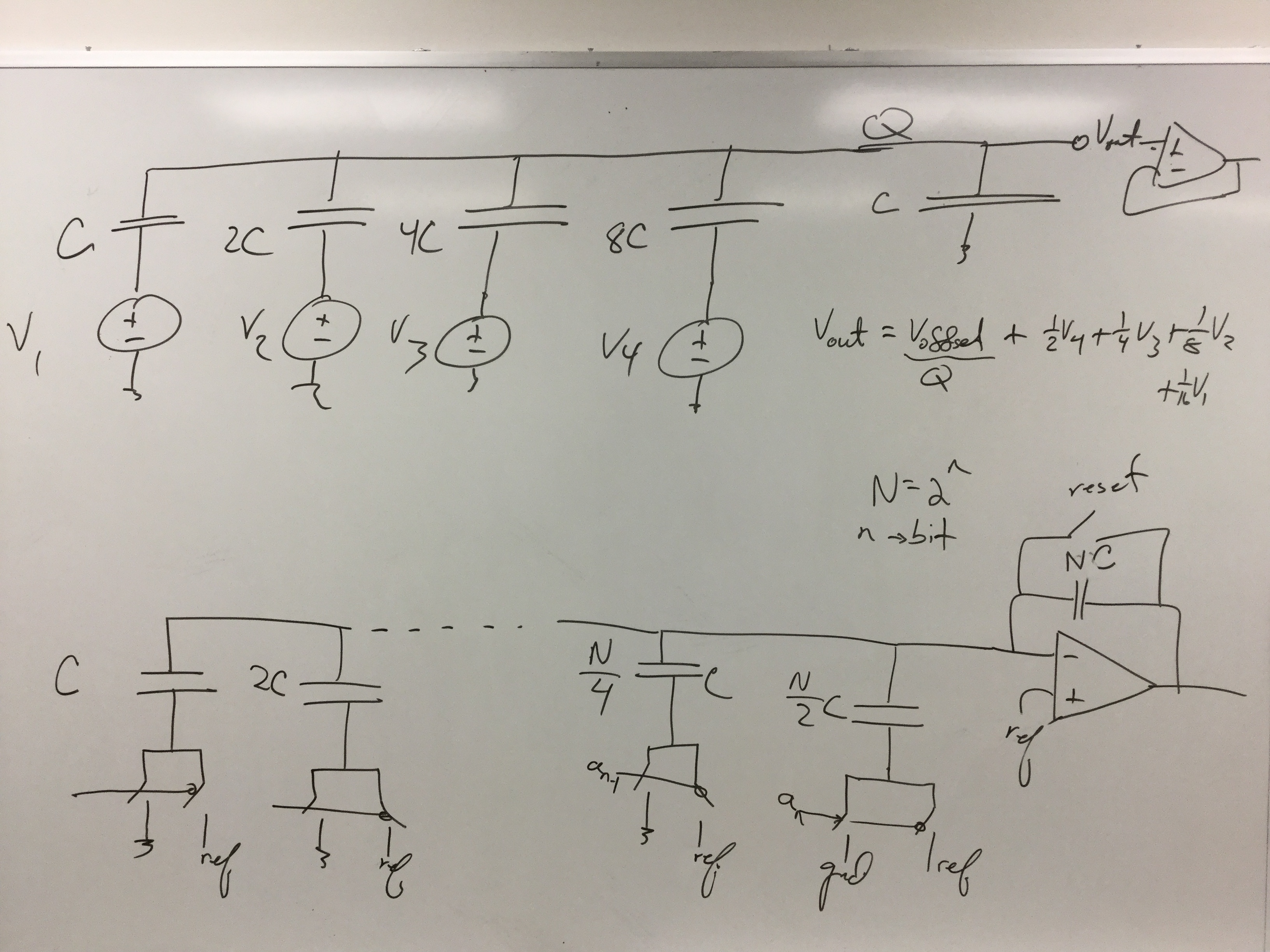
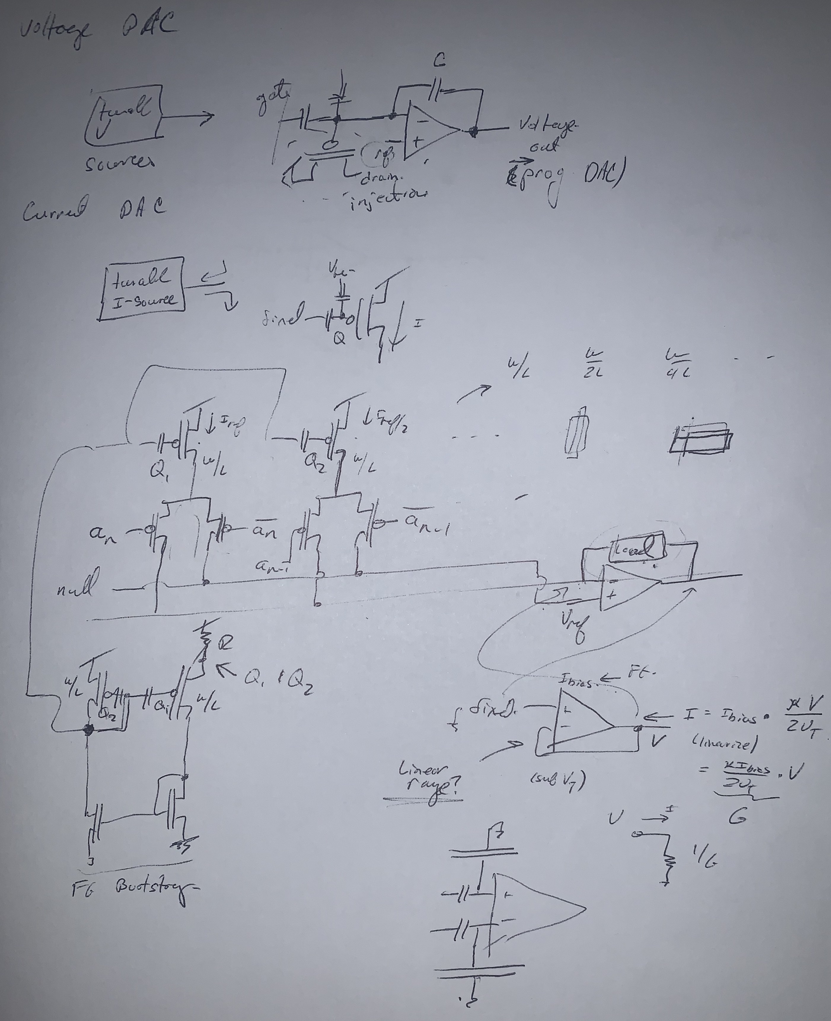
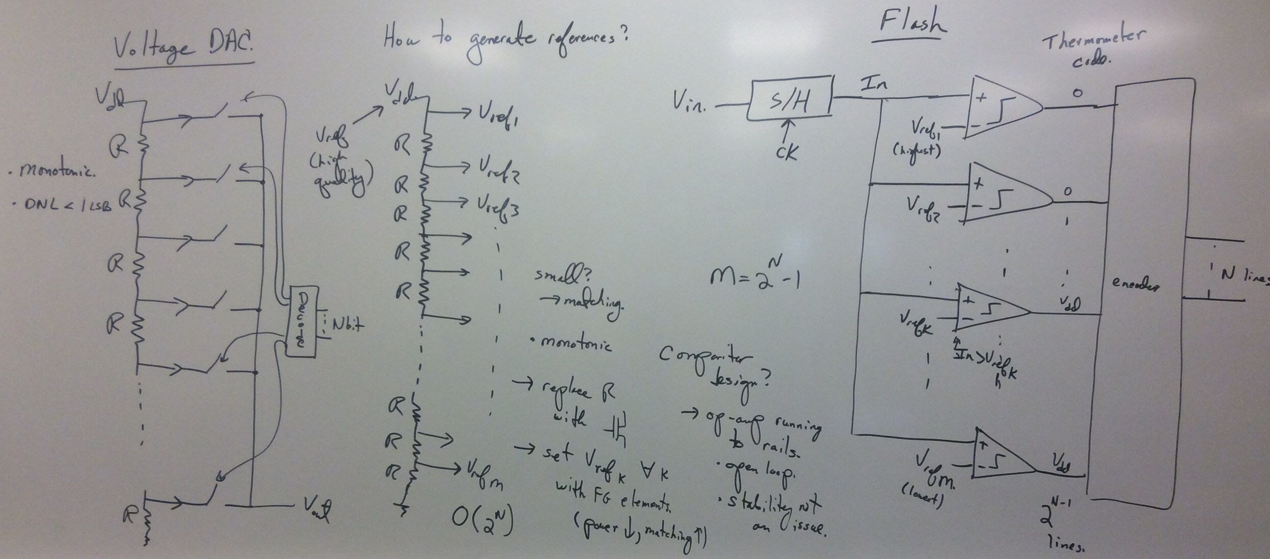
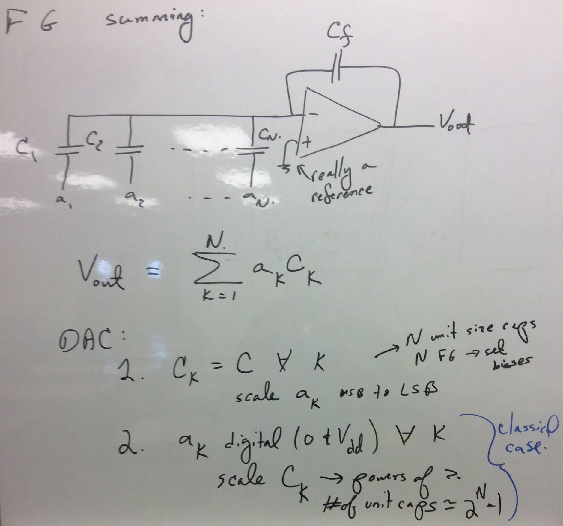
System Design 2: A Voltage Output DACThis system design will require making a 12bit Voltage-Output DAC. The DAC must be able to drive at least a reasonable capacitive load (like using a typical MOSFET amplifier), typical of other MOSFET circuits.
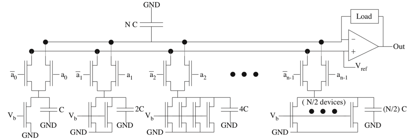
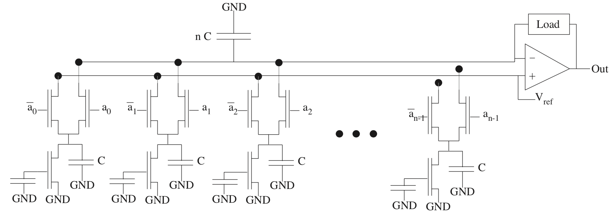
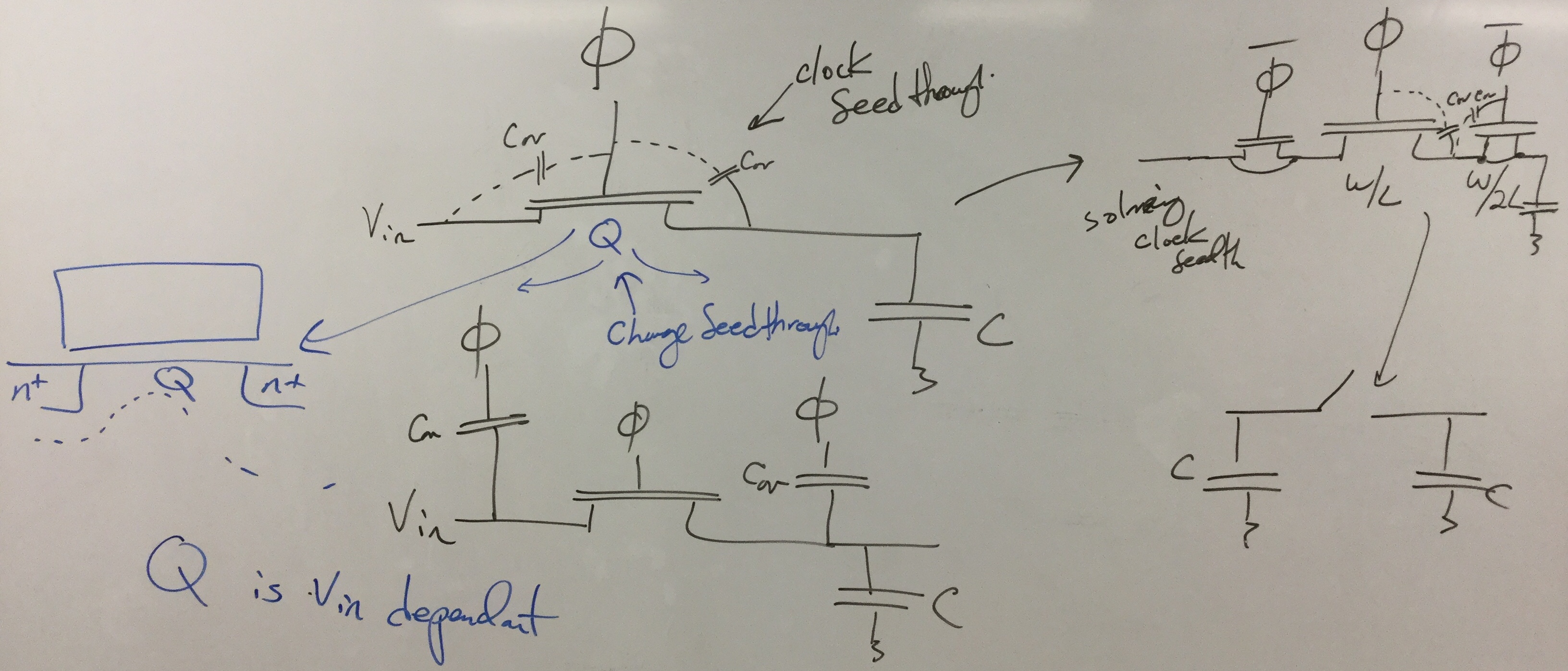
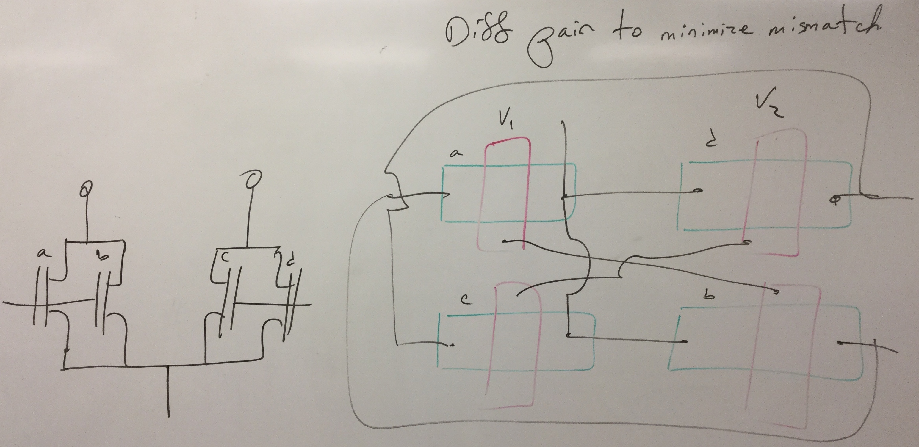
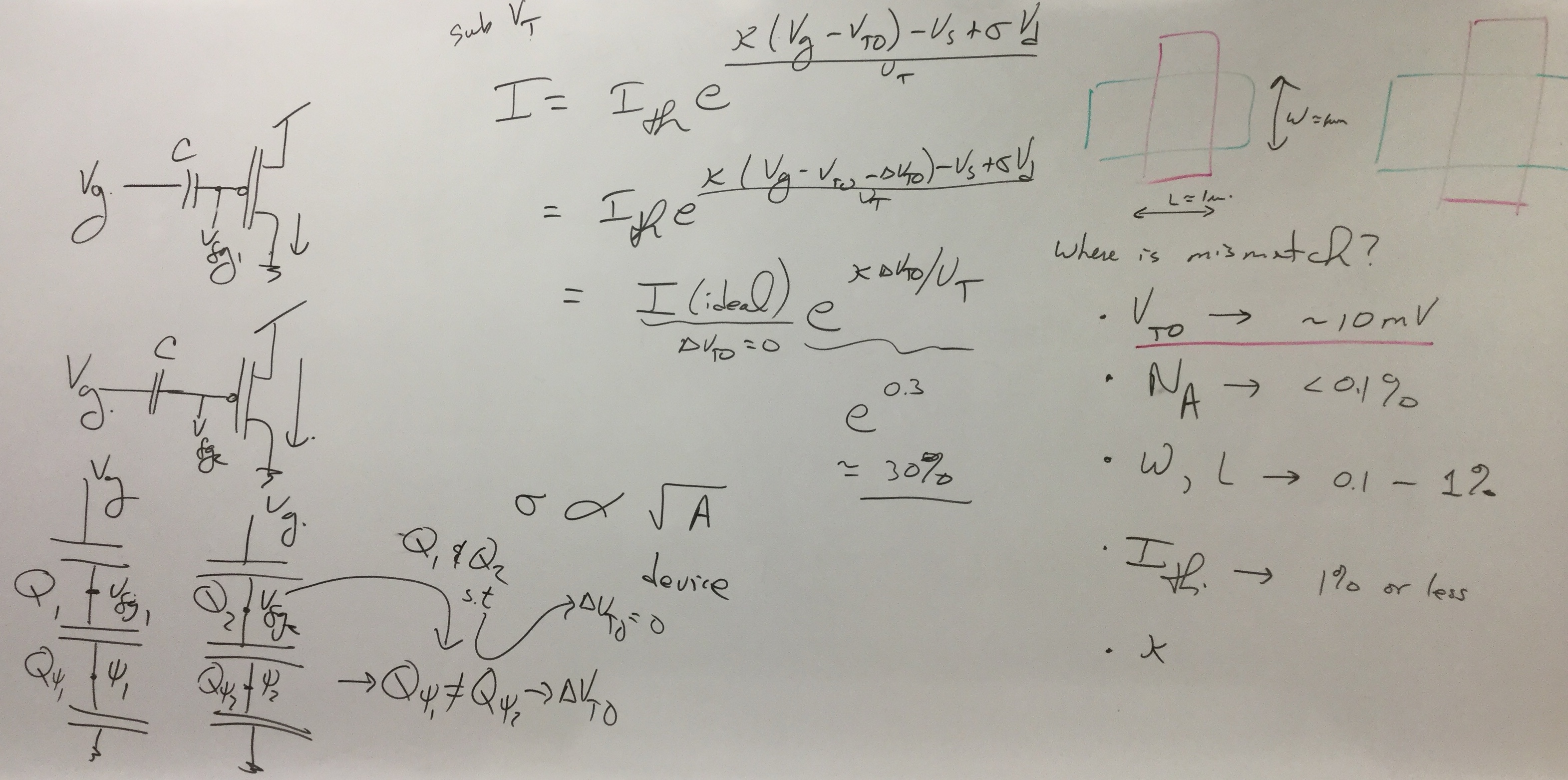
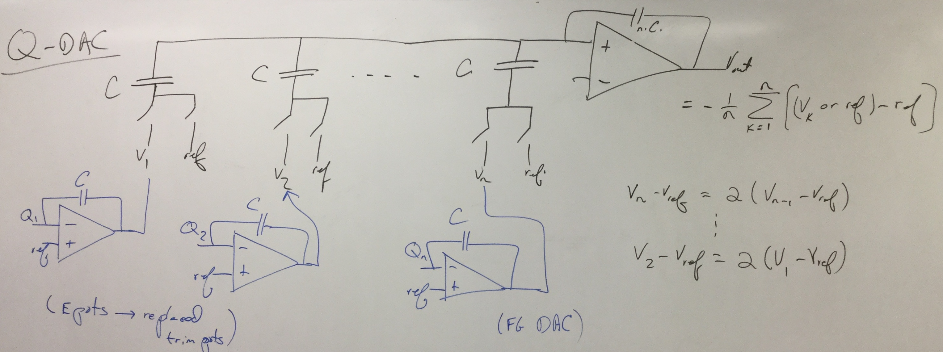
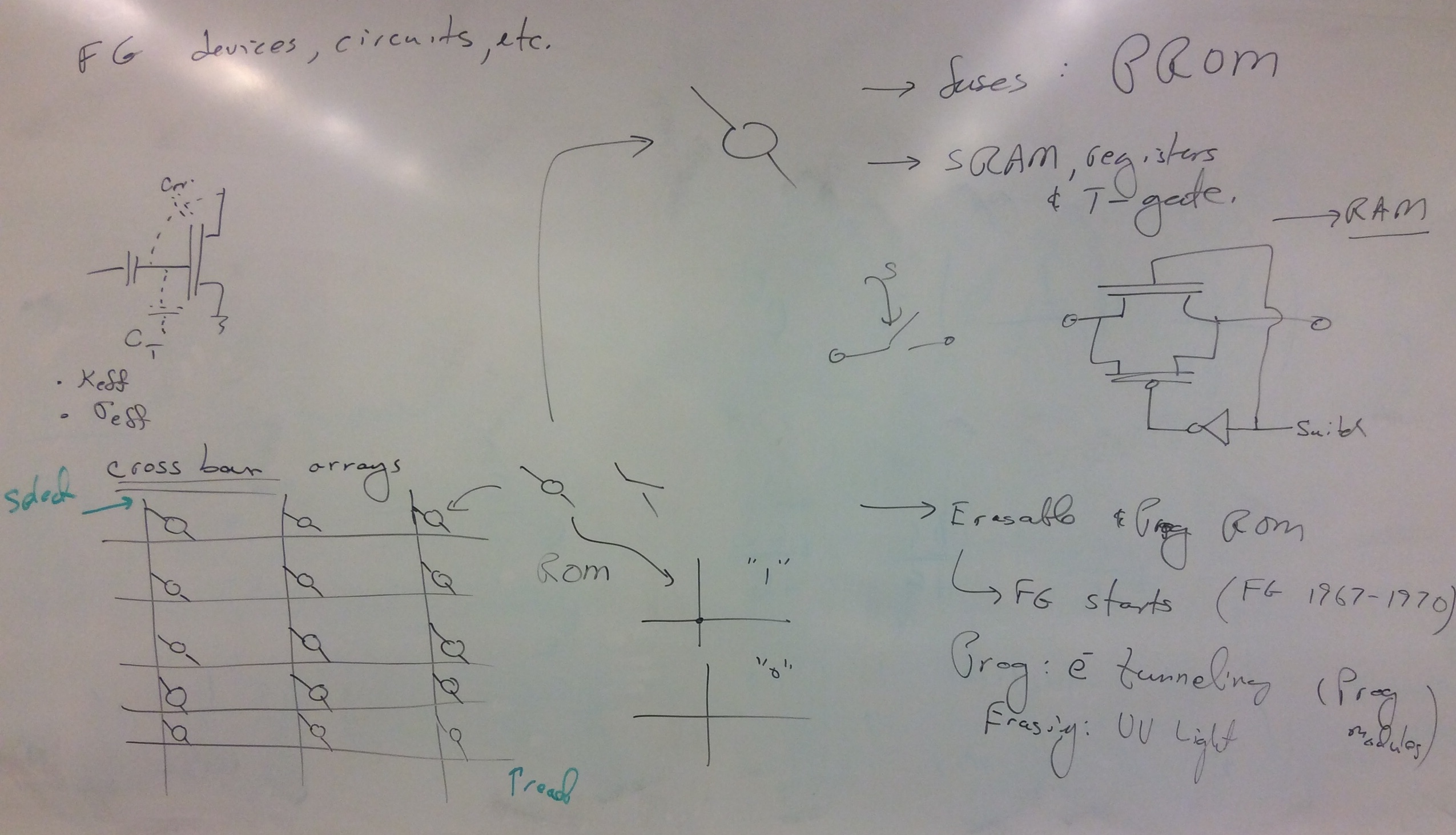
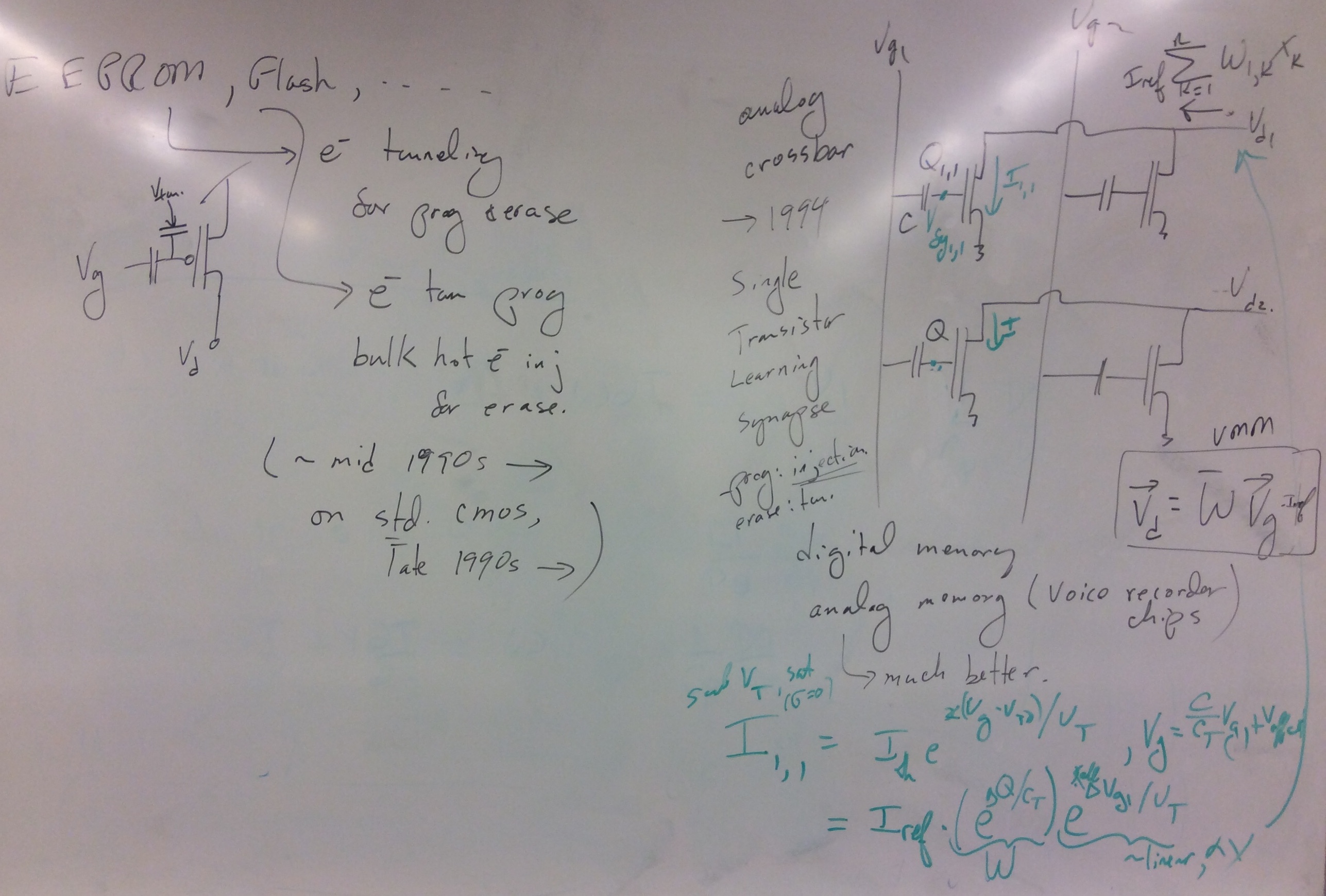
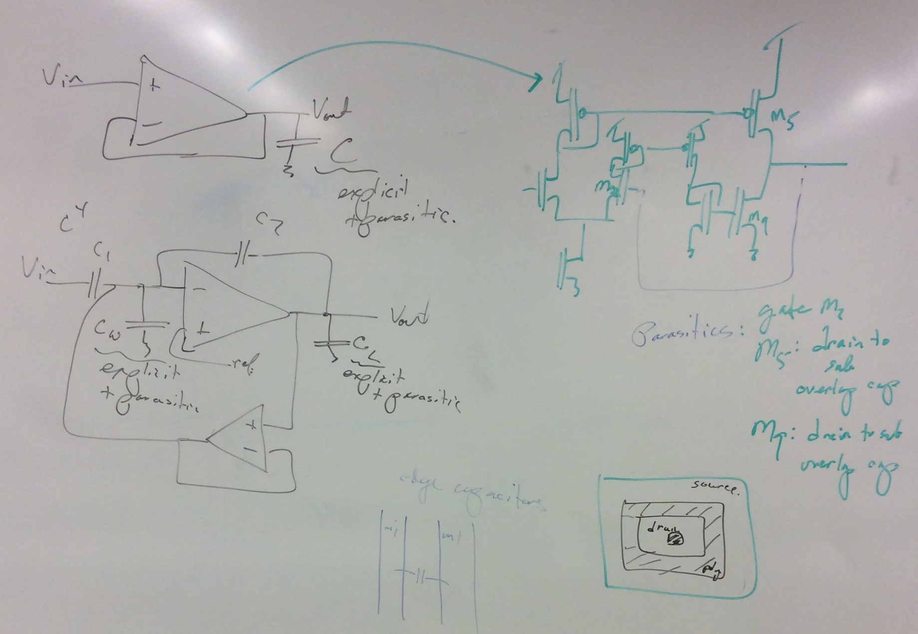
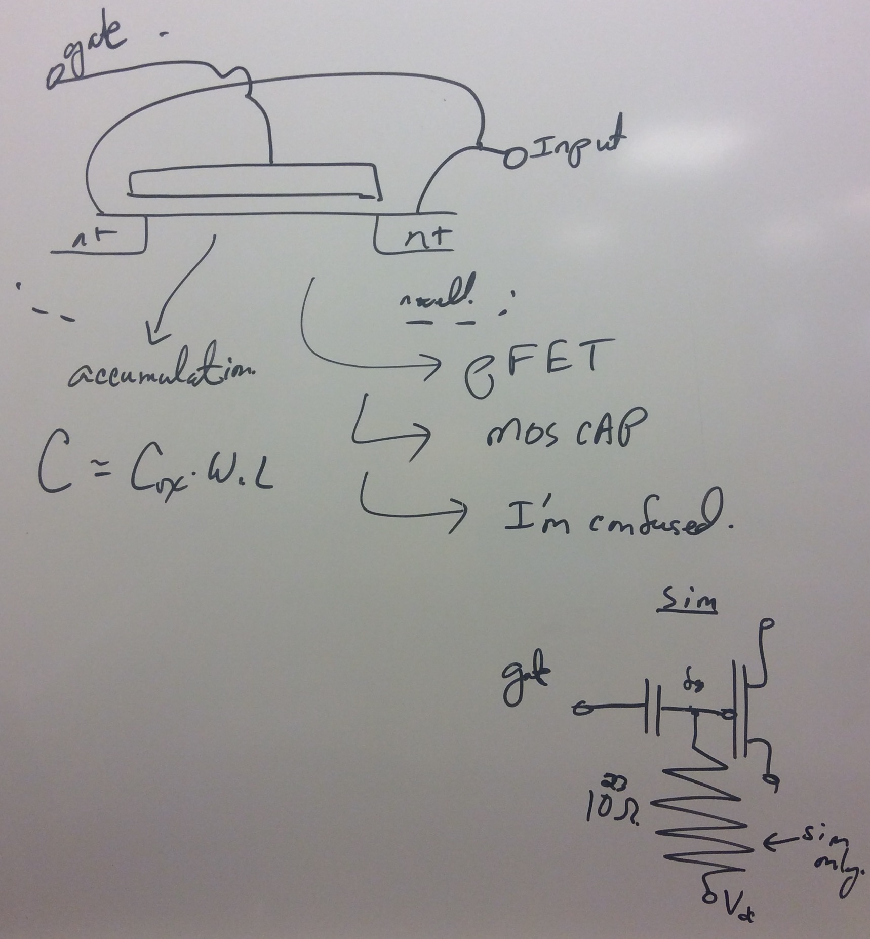
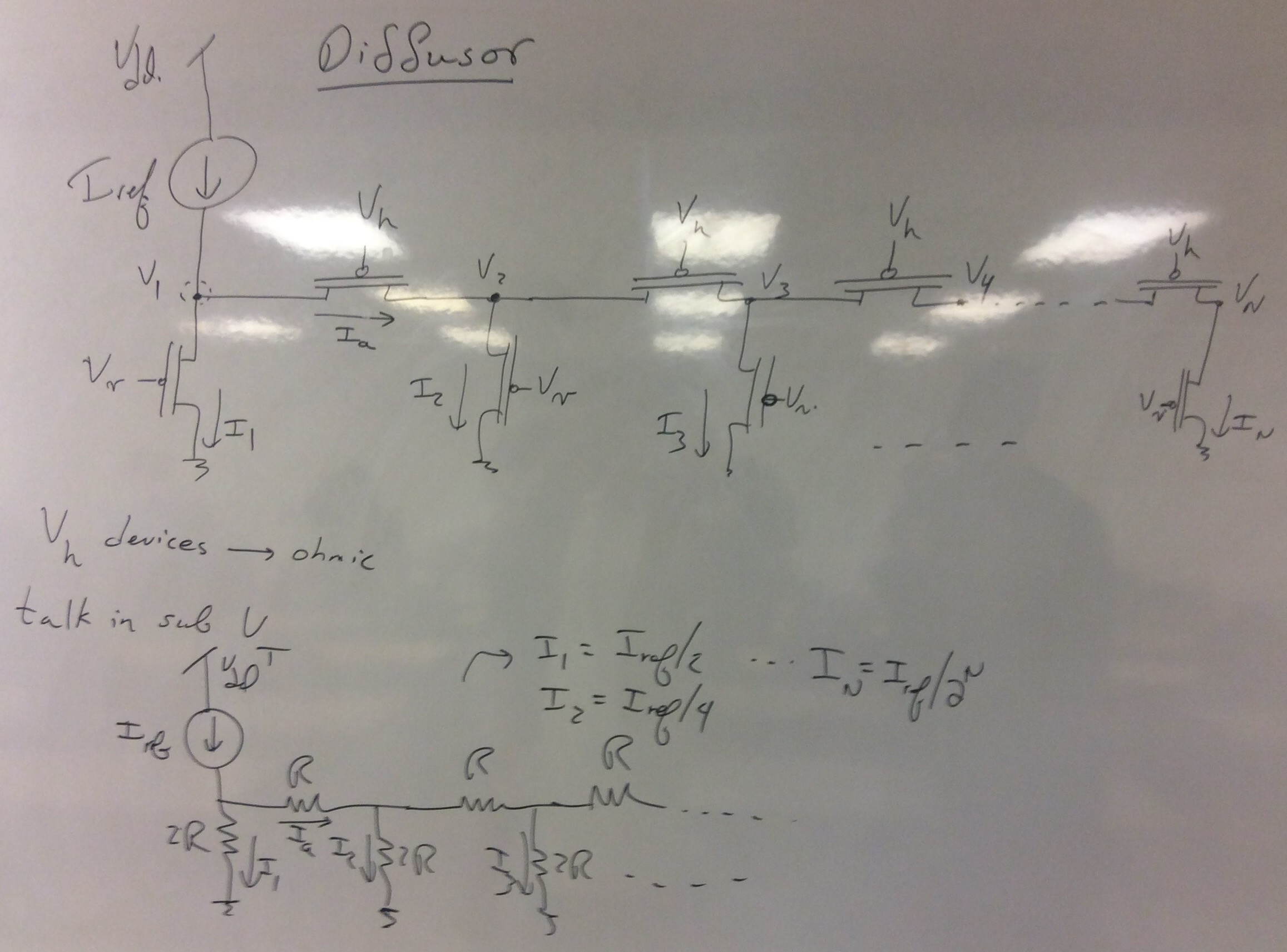
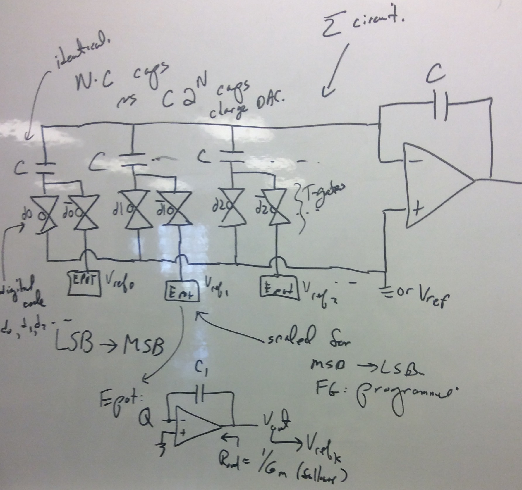
Fig. 2: Two potential classical based DAC structures. (a) A voltage-topology (charge DAC) voltage-output DAC. (b) A current-topology voltage-output DAC. Your particular topology that you would use is flexible for the design. Area required for the in-pitch design is an important grading criteria. Mismatch is an essential discussion in your design. FG approaches are acceptable for this approach assuming you handle the resulting infrastructure for programming. Two sample potential classical DAC structures are shown in Fig. 2, and FG DAC structures are shown in Fig. 3. The sampling rate is given specifically to each group.
Fig. 3: Two potential FG based DAC structures, one based on switching voltage elements, and one based on switching current levels. (a) A Floating-Gate voltage-topology voltage-output DAC. (b) A Floating-Gate current-topology voltage-output DAC. Layout items to submit :
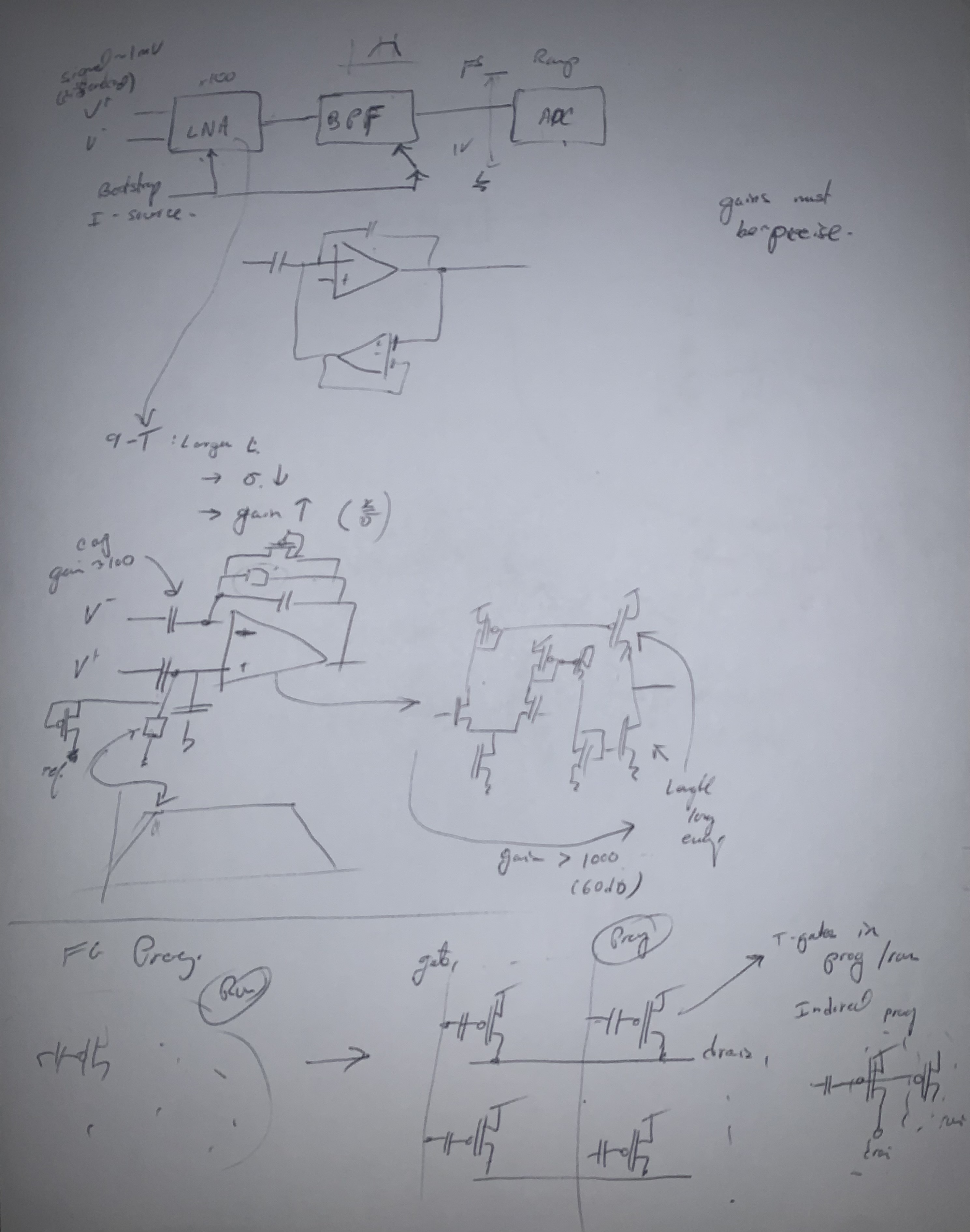
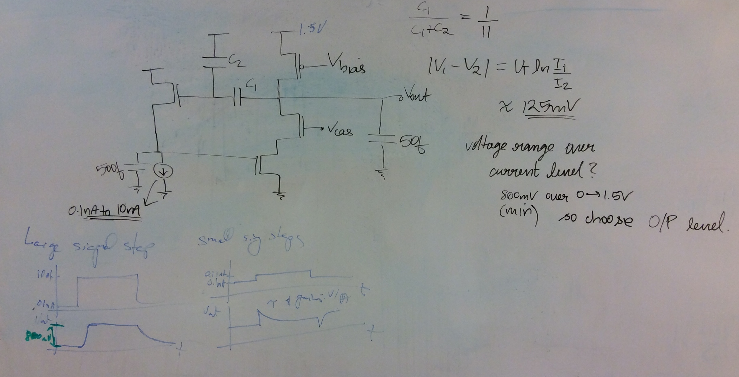
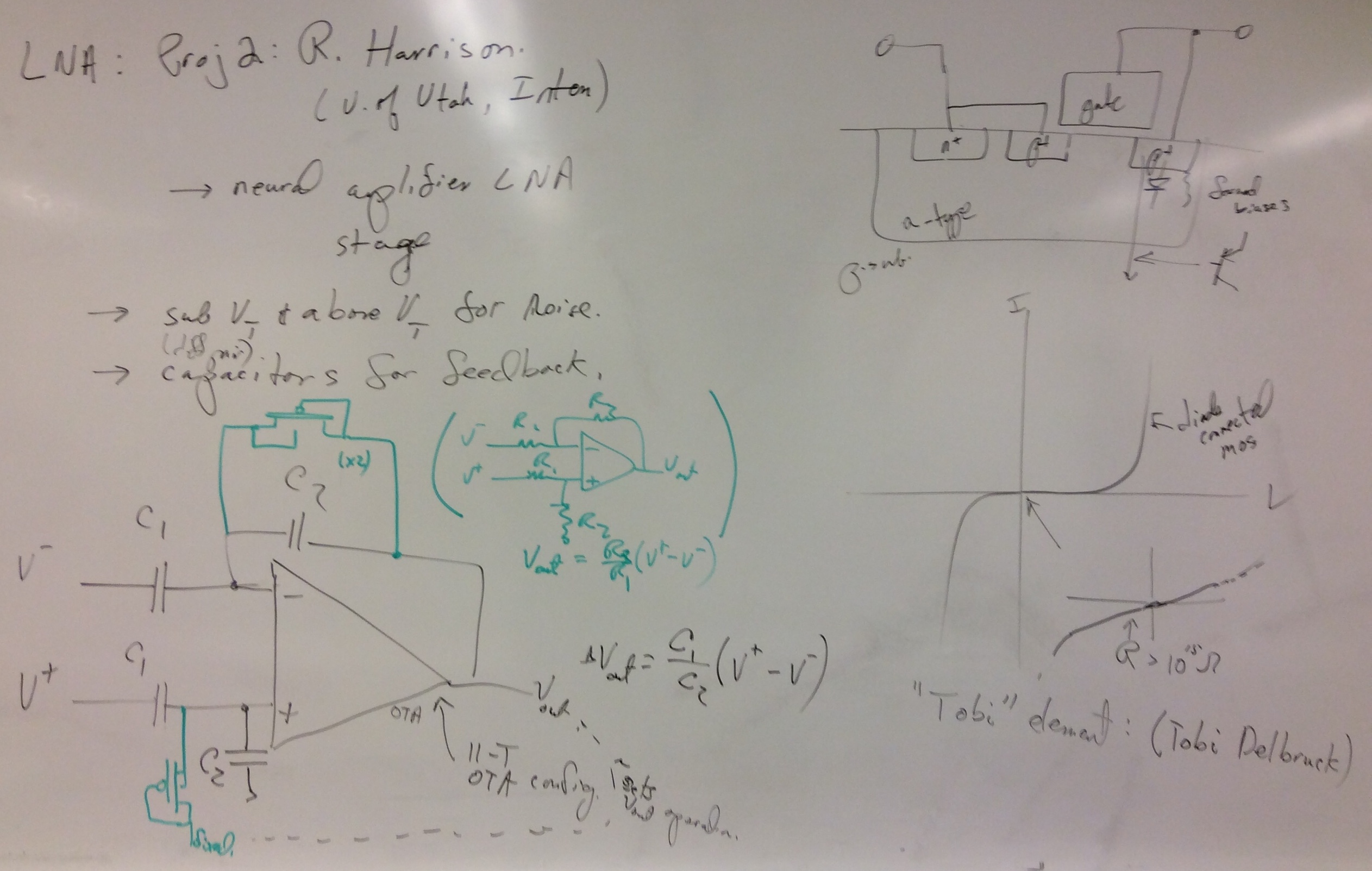
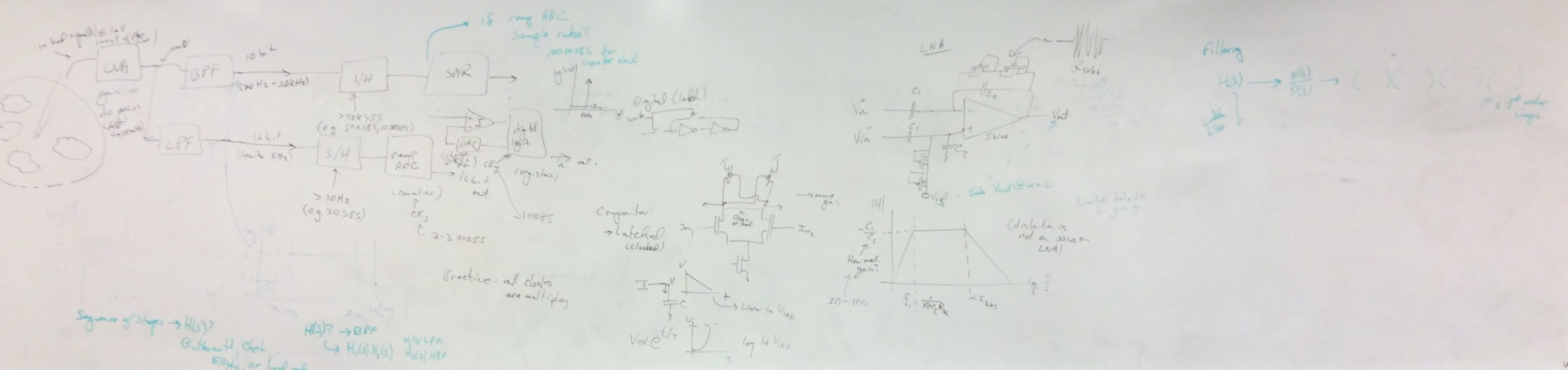
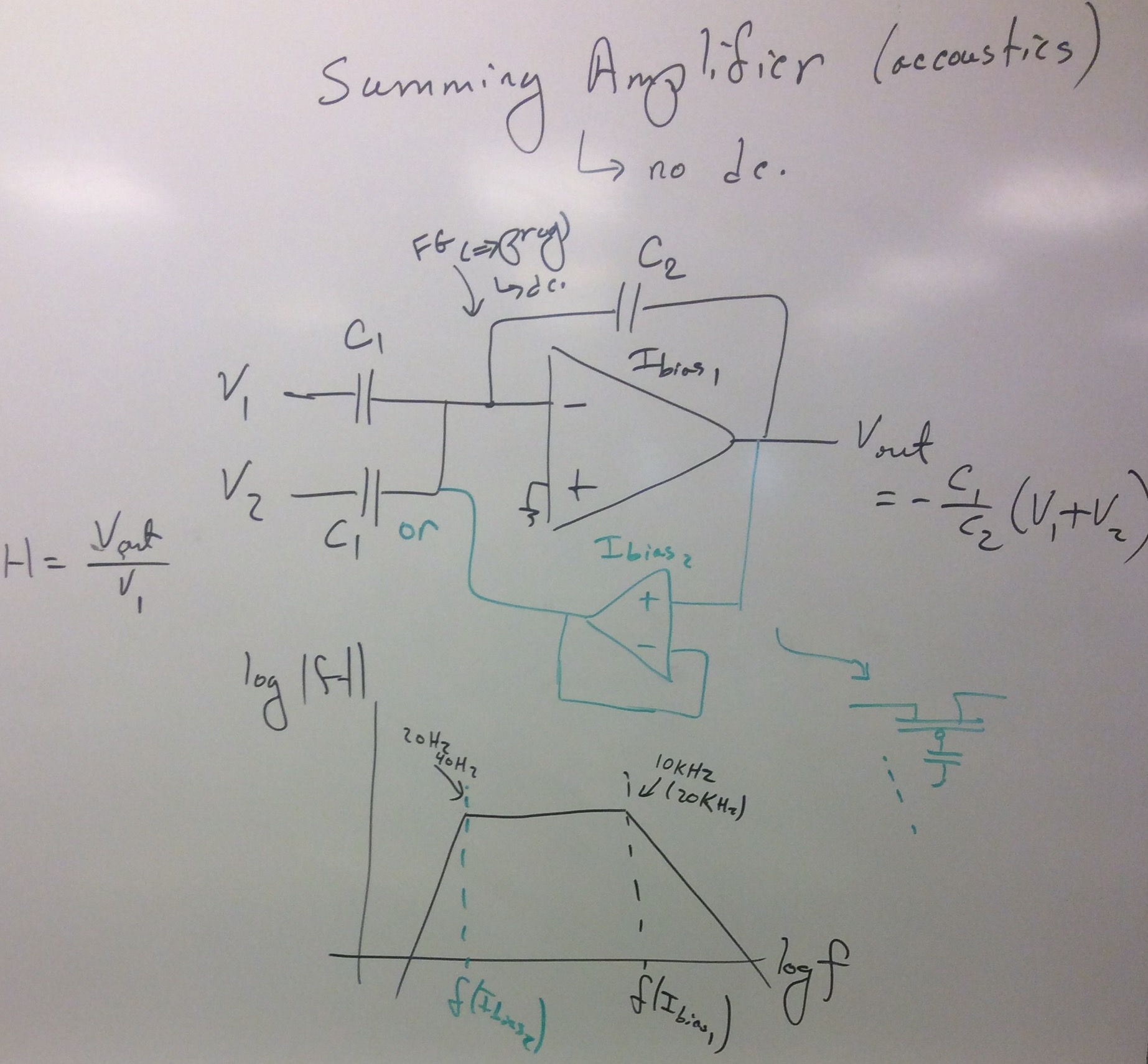
System Design 3: A Front-End Neural Sensing ArchitectureThis system will build a system for handling neural sensing measurements, where typical input signals were 1mV or less. Front-end Low-Noise Amplifier The front-end amplifier would be a version of the neural amplifier, as capacitive feedback around a low-power amplifier.
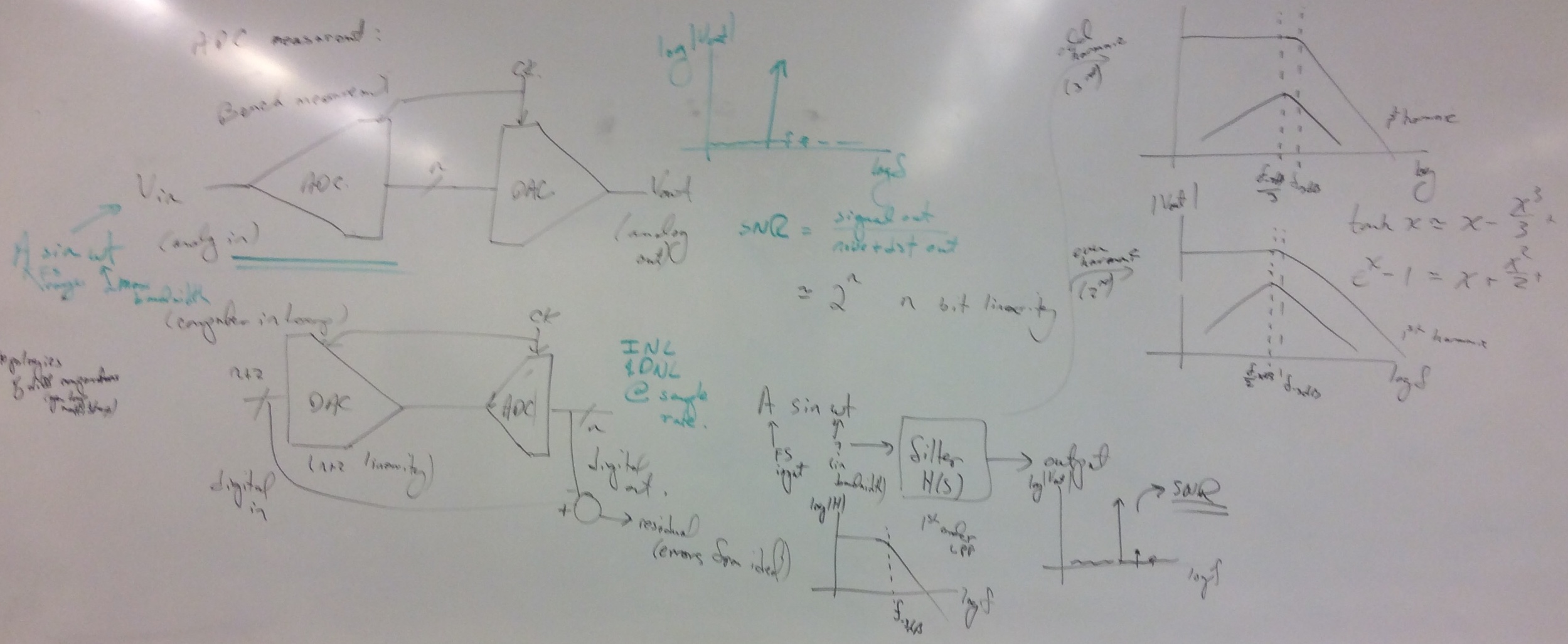
Amplifier Gain and Filter Stage: This amplifier stage provides enough gain and filters the output such that 1mV signal is the full-scale range of the ADC stage. The frequency range for gain 10Hz to 5kHz frequencies. Output SNR must be at least 60dB that should include noise and distortion. ADC Stage: The ADC computation must be able to take a signal in the range (e.g. 300mV to 1.5V) and convert it to the desired resolution using a ramp ADC for a 12bit resolution and linearity. Linearity should be demonstrated in terms of INL and DNL measurements at the maximum frequency of the ADC operation. Sample rate requirment is what is necessary to fully reconstruct the original input signal. Layout items to submit :
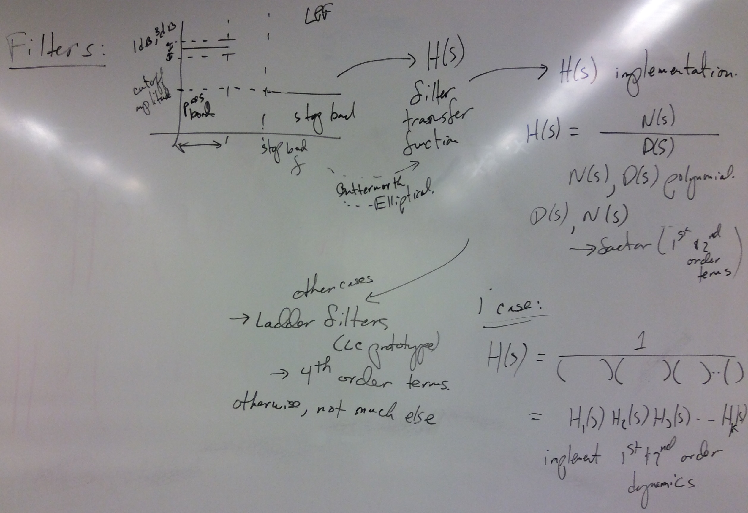
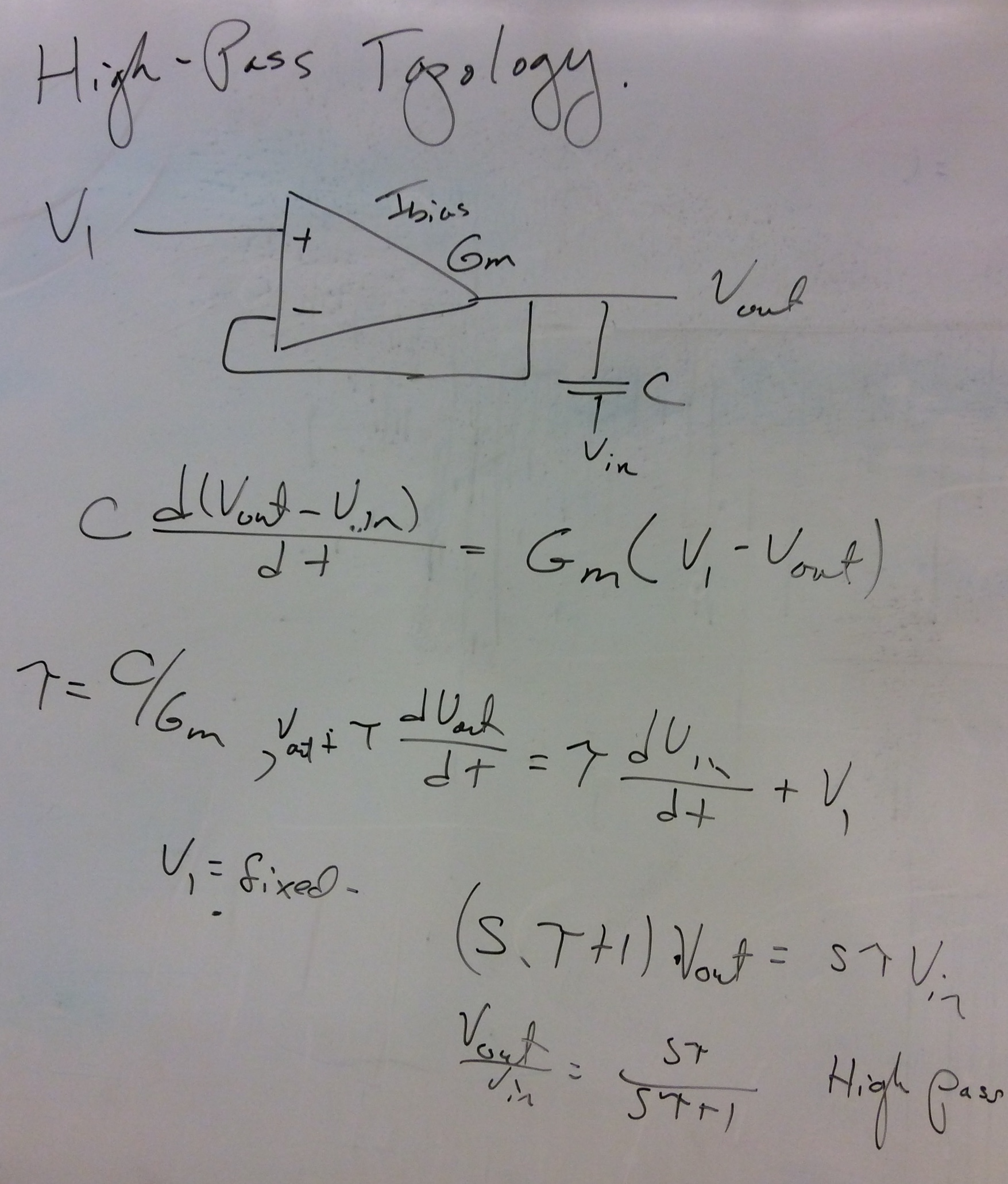
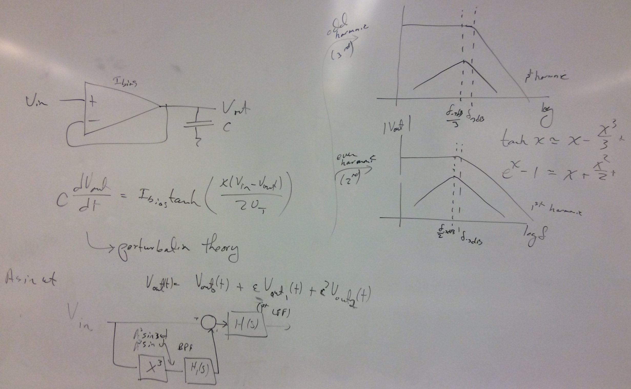
Previous ApplicationsApplication: Neural Probe Front-End Architecture (2019)For all designs, optimizing power consumed as well as area are critical for both designs. The power supply for the IC will be 1.5V, and will use the same process we have all semester. The layout and post-layout simulation for this project is essential. As this design is a physical design, you should be aware of design mismatch on your IC, where appropriate. Dealilng with mismatch is a critical graded component. You should discuss the effect of temperature on your design, if it is present at all. You effectively do not have any explicit inductors or resistors, other than a single resistor for setting current in a bootstrap reference. This project focuses on build an analog system design for sensing neural recording. Typically we would want many of these probes, but we will concentrate on the design of a single input for this problem. In these applications, power is really critical, since often the power is wirelessly inductively coupled to the circuit, and as a result, we want to use as little power as required. Front-end Circuitry and Filter StageWe are looking at typical input signals that are roughly 1mV and we want an SNR of 60dB. We would want an LNA with 40dB of gain to bring the maximum signal to 100mV, which can be handled and not creating that much distortion. The DC signal, at the frequencies associated with changes over minutes and hours, could change significantly (1-100mV input change), and must be eliminated from the incoming signal at the LNA stage. We expect the output signal into the next stage is a peak of 100mV, with the output SNR of this stage being 60dB. We don't expect nonlinearities to be an issue for this stage.We will want two different signal paths coming from the LNA signal. One path is for identifying the action potentials, so looking at frequencies above 10Hz and upto 20kHz frequencies. The second path is for identifying low frequency waves going through the neural tissue, so we are looking at frequencies of 5Hz and below. We expect both of the filters to output a signal that is for a maximum input to be 1.0V peak to peak within the power supply. The signal must be away from the power supply rails by 200mV. The input from the LNA won't necessarily have a well defined DC point, so your filter must handle these issues. This issue won't be a problem for your bandpass filter. The input common mode range should be from 200mV to 1.3V, because the DC isn't defined and can vary. You don't need rail to rail input stage for your OTA, but a reasonably wide input range is important. Filter stage passband would have 1dB ripple with -20dB down from the one octave below (stopband). In terms of gain, you should realize your starting input signal could be as big at 100mV (pk-pk). Your output signal will be max of 1.5V (pk-pk). Therefore your gain needs to be 10 between input and output of your filter, although you can tradeoff your gain with the LNA stage where helpful. Your bandpass filters might have intrinsic gain depending on the topology you pick. Distortion for a 100mV input sinusoidal signal in the band of interest should be at least -40dB below the primary harmonic for a two-tone test. The SNR needs to be 60dB SNR from the output filter. Because of distortion, the amplifier will multiply these signals internally, and you will see their products in the spectrum. The distortion measurement in this case is whats called a two-tone test which is used to test intermodulation. It's where you input a fundamental sinewave and another sine wave of a different frequency, but close to the fundamental (two sine sources in series), both of the same magnitude, and look at the output spectrum (say an FFT). You want to make sure that when you look at the spectrum (in dB) on the output that your w1 and w2 signals are at least 40dB above the harmonic signals. You will use the largest signal possible at the input (i.e. 100mV into the filter stage) to see what intermodulation products get generated such that they're above the noise floor. If you use a really small input, then you won't see the products. Depending on the bandpass filter topology chosen this spec should not be too difficult, and there are circuit design aspects that can be modified to get more linear range. ADC Stage:The ADC computation must be able to take a signal in the range from 200mV to 1.3V and convert it to the desired resolution:
Application1: Front-end System design for Neural Recording
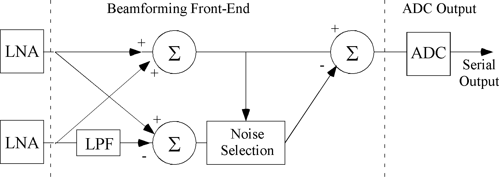
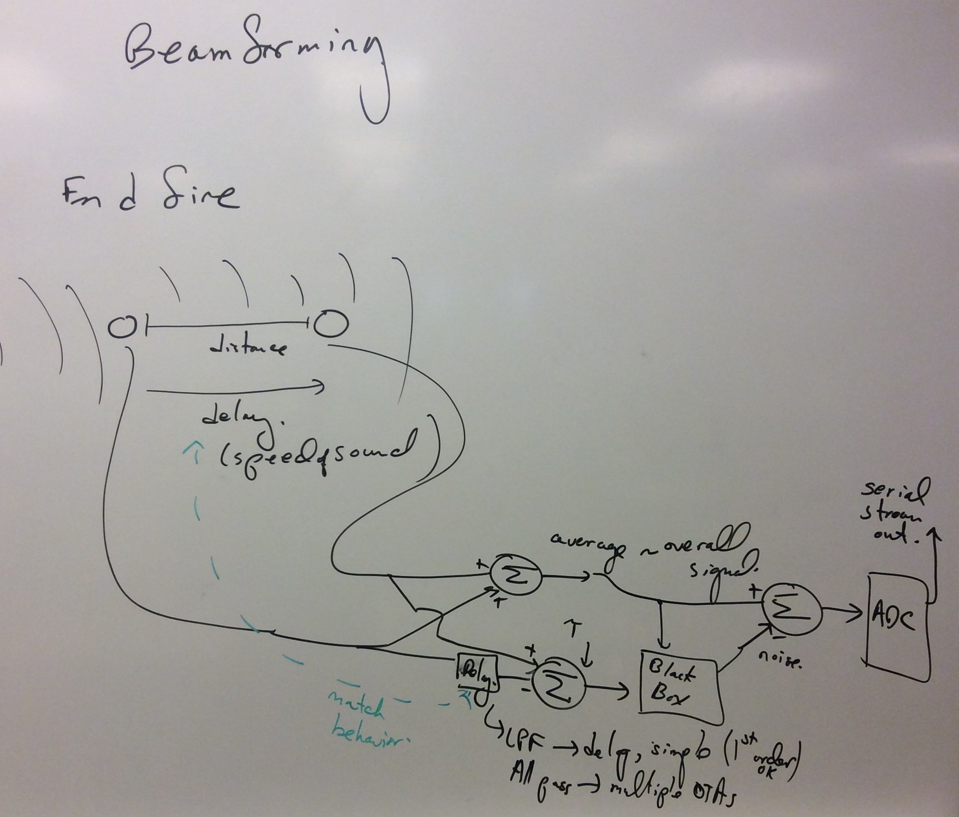
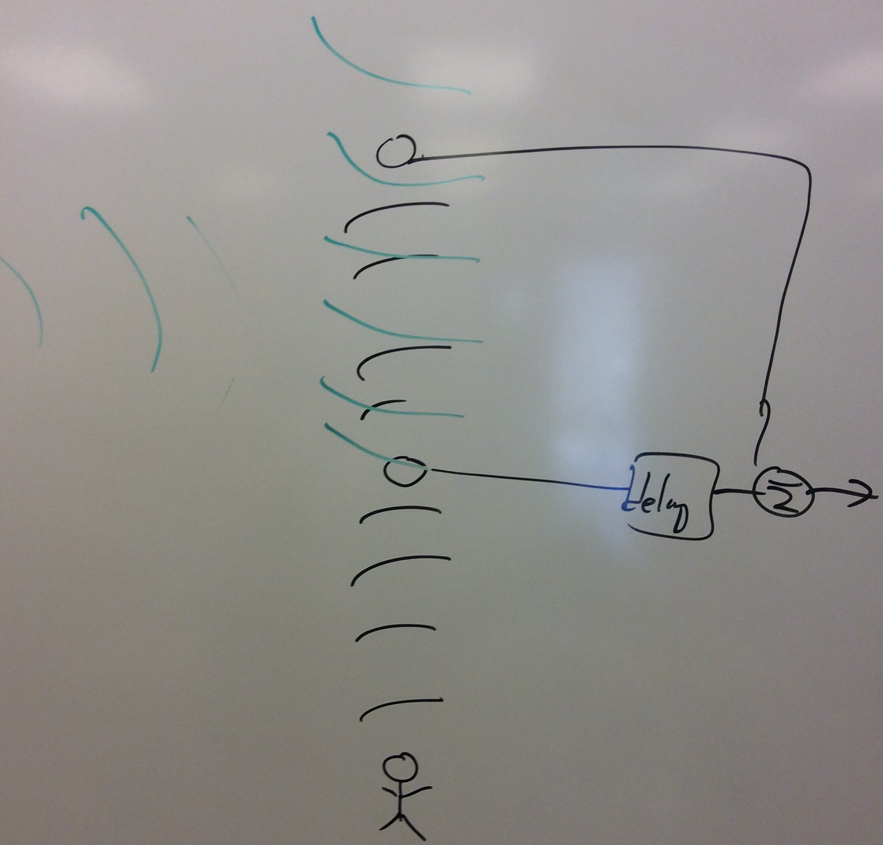
Figure 1: Basic Two device beamforming architecture for two sensors in an endfire configuration. The goal of this project is to build the accoutic front-end signal processing for a two-input beamforming system as part of a wireless headset. Beamforming is used to improve the SNR of the transmitted signal. The beamforming described here reduces the background noise by placing a null in a non-preferred direction. Figure 1 shows the architecture for this system. The output quality needs to be good enough to be used for Voice over IP quality, Your inputs start from Analog capacitive-sensing LNA modules, originally developed by S.Y. Peng, et. al (in our circuit references). Area must be minimized because the circuit will fit ideally in an area containing the two microphones and the resulting circuit. Power must be minimized because it will be in a power constrained environment (a wireless headset) where one does not want to charge the battery often. This project will have two parts. One group (team 1) will build the beamforming front-end circuitry and one group (team 2) will build the output Analog-to-Digital Converter. Beamforming Front-End CircuitryThis circuitry will primarily be selecting Assume the input LNAs give 12bit SNR outputs or higher for your consideration. You will want to be able to select between at least two null positions. Your output signal must be
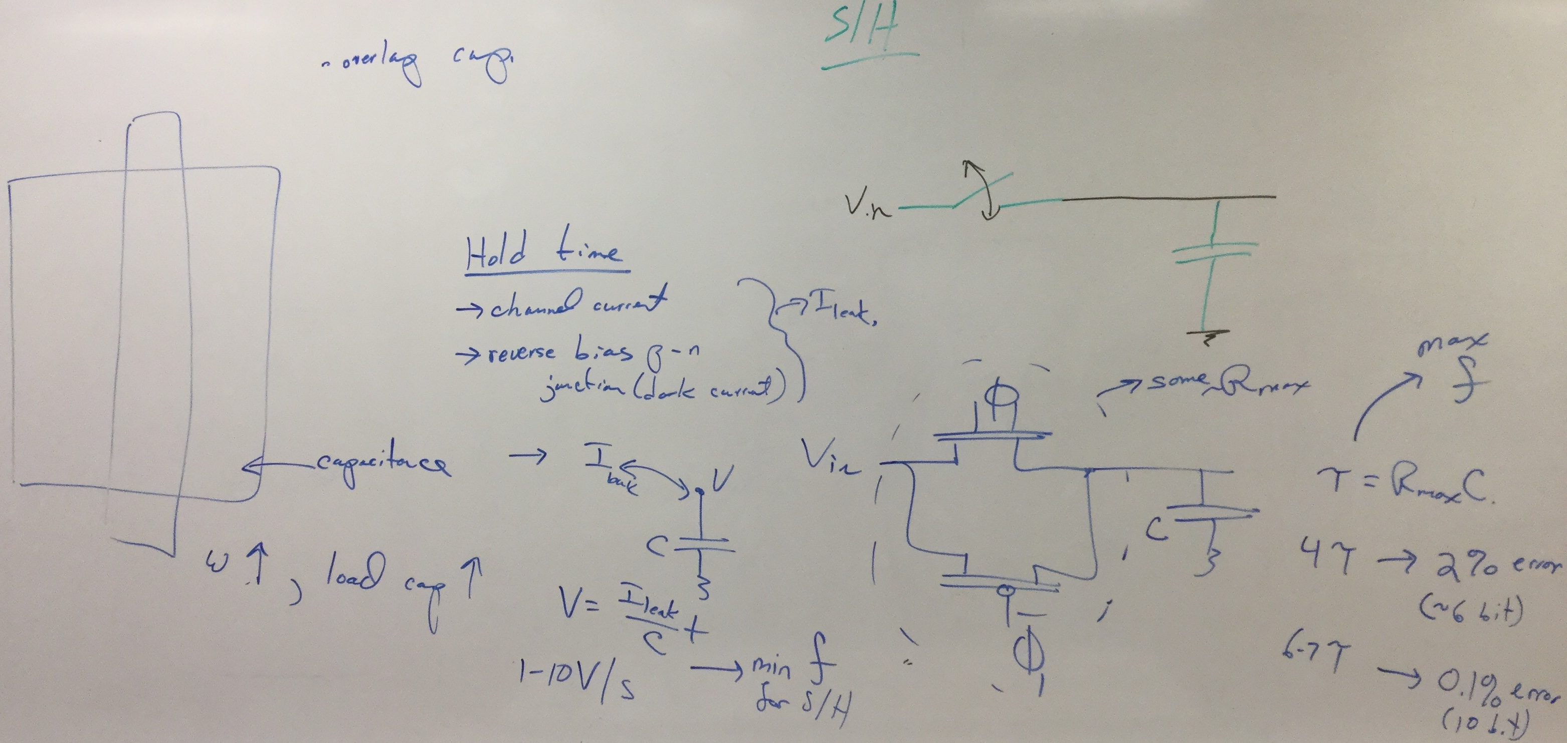
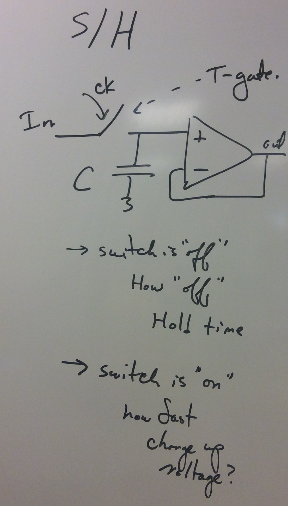
ADC DesignYou will need to build an ADC to convert the output waveform to a digital form that could be transmitted by a standard zigbee module. The output signal will be a serial bit stream of the resulting bits, ideally an SPI bit stream. You will need an appropriate S/H stage before your ADC.
Application 2: Ultrasound In-vivo Imaging ReceiverThe goal of this project is to build a front-end analog signal processing for a single channel of an ultrasound receiver used for in body (In-vivo) imaging. For the particular distances to measure, the ultrasound carrier frequency of the simulation and measurement is 30MHz. The resulting output bandwidth will be 1MHz. Area needs to be minimized because of constraints for an implanted device, potentially in small areas like blood vessels. Power must be minimized since getting power into the body can be a challange (battery or wireless) and the implant should not affect the surrounding temperature. This project will have two parts. One group (team 3) will build the analog front-end electronics, and one group (team 4) will build the Analog-to-Digital Converter. Front-end designThis design will take the initial 30MHz front-end signal and create a bandlimited 1.5MHz signal.
ADC DesignYou need to design an appropriate Sample and Hold for the input of the ADC. You need to design the parallel output voltage register that will have the resulting ADC signal. You will need an appropriate S/H stage before your ADC.
|