|
| Date | Class Topic | On-Line Lectures | Reading Material | White Boards |
| Jan 9 | Neuromorphic Overview |
C. Mead ACM
1997
|
Mead Neurmorphic Engineering (1990), FPAA Scilab/Xcos tools | |
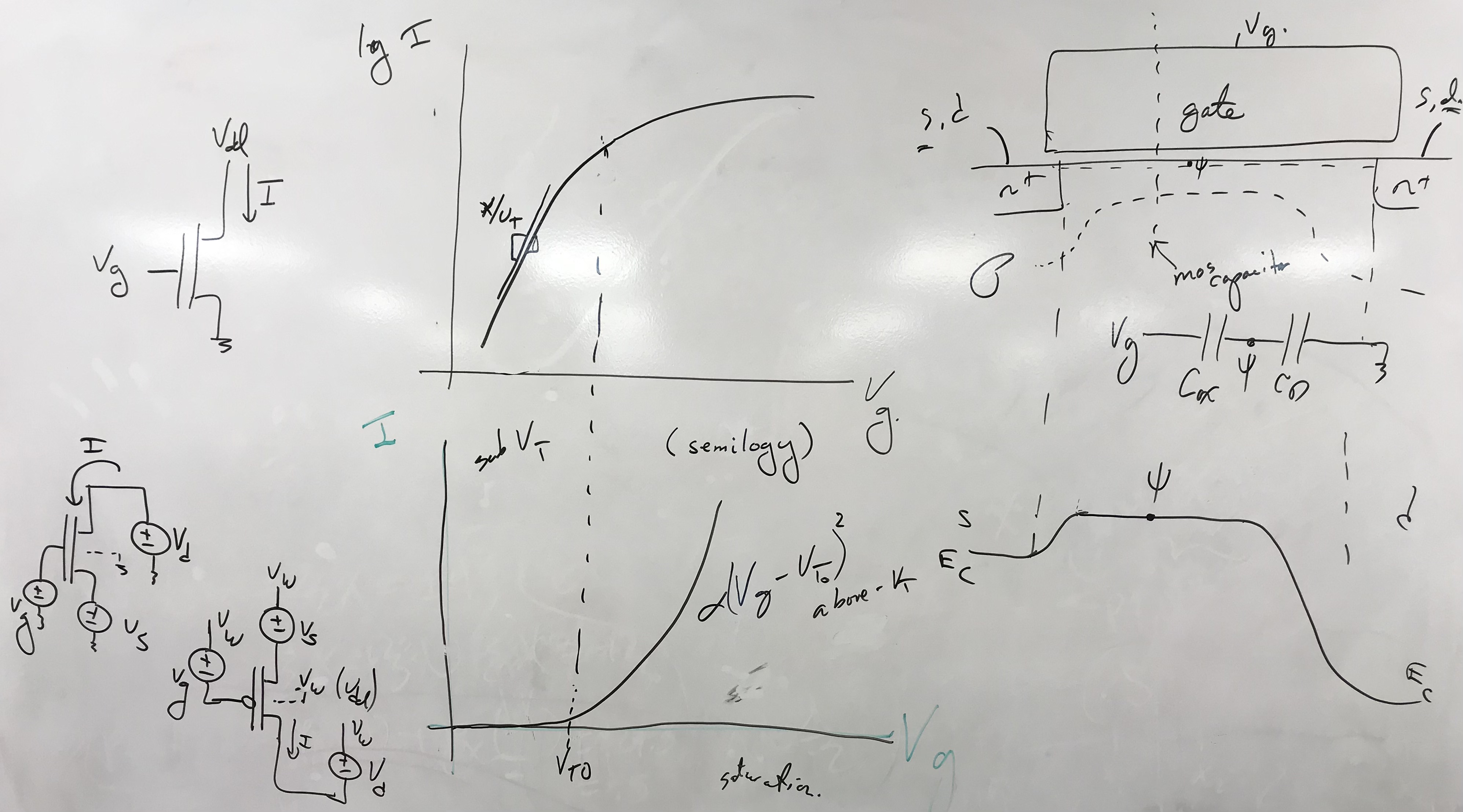
| Jan 11 | MOSFET Devices |
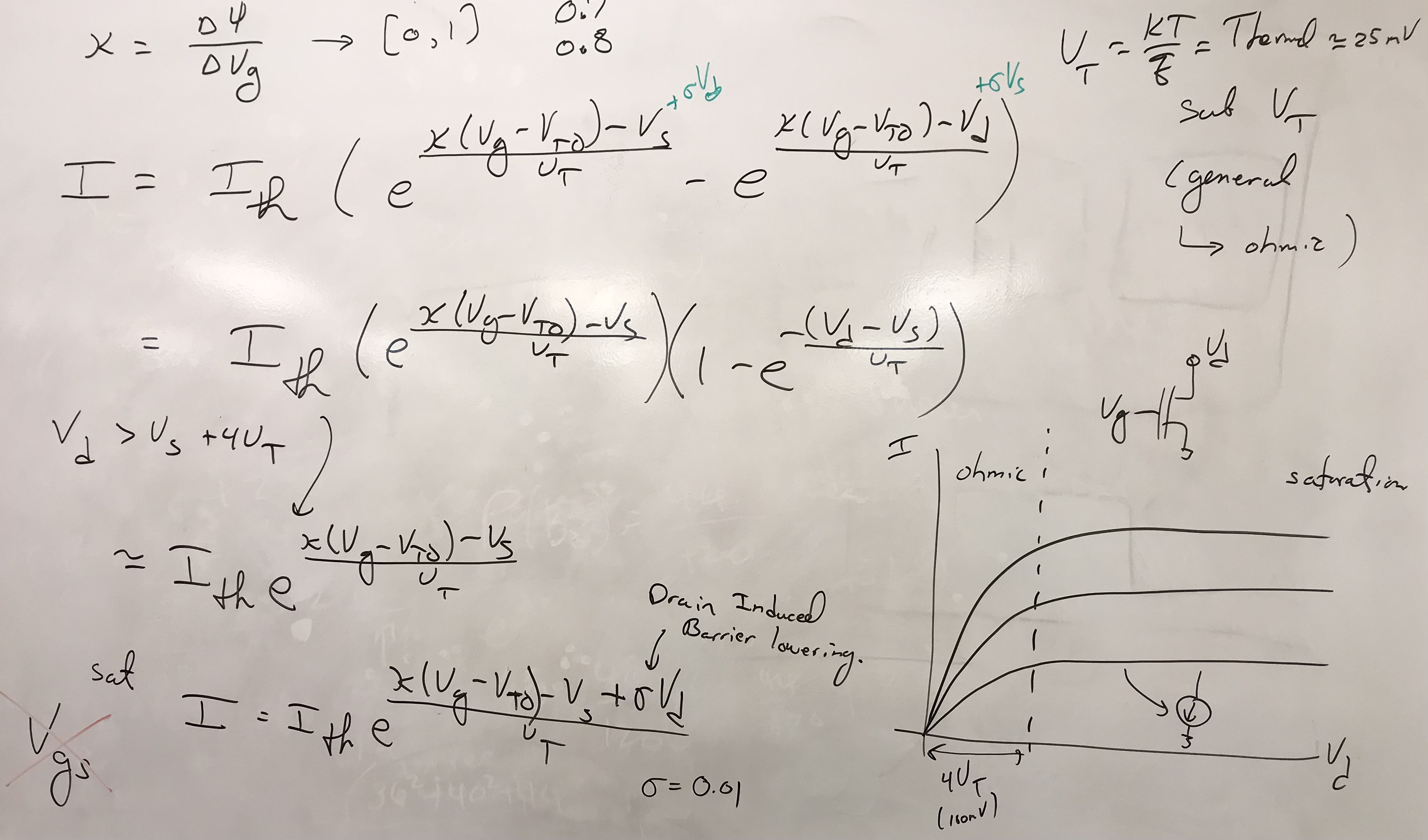
Semiconductor Barrier, MOSFET basics, MOSFET Subthreshold Equ "sigma" = VA / U_T should be "sigma" = UT / V_A, Subthreshold Derivation, FPAA Tools |
Device Physics(Chp.2) SubVT Transistor(Chp.3) FPAA Overview FPAA Tool Overview Scilab sim (level=2) Remote FPAA System . | |
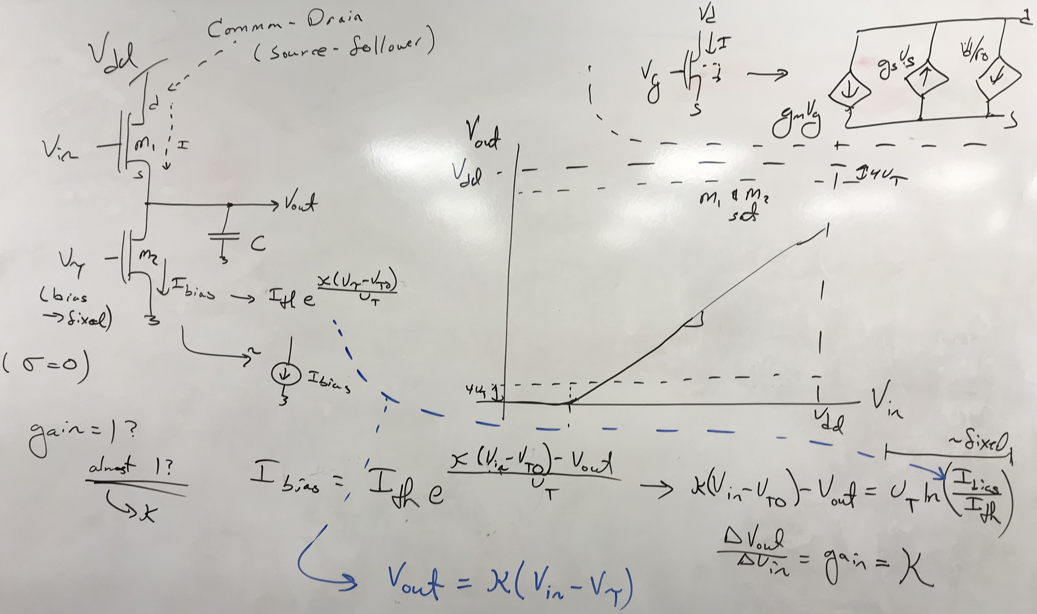
| Jan 16 | MOSFET Circuits I |
MOSFET = Current Source, DIBL Modeling, One-T Circuits Single-T Amps Pair Diff V Amplifiers FPAA Tool Demo Tool Example LPF SoC FPAA Infrastructure |
SoC FPAA IC Transconductance Amplifier (TA) (Chp.5) DIBL and "sigma" SubVT transfer functions | 1, 2, 3, 4, 5, 6, |
| Jan 18 | MOSFET Circuits II |
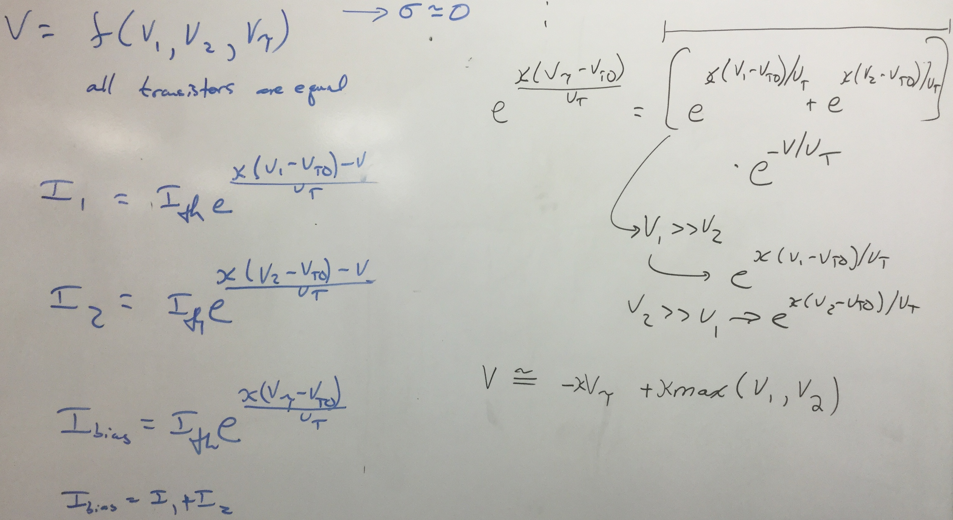
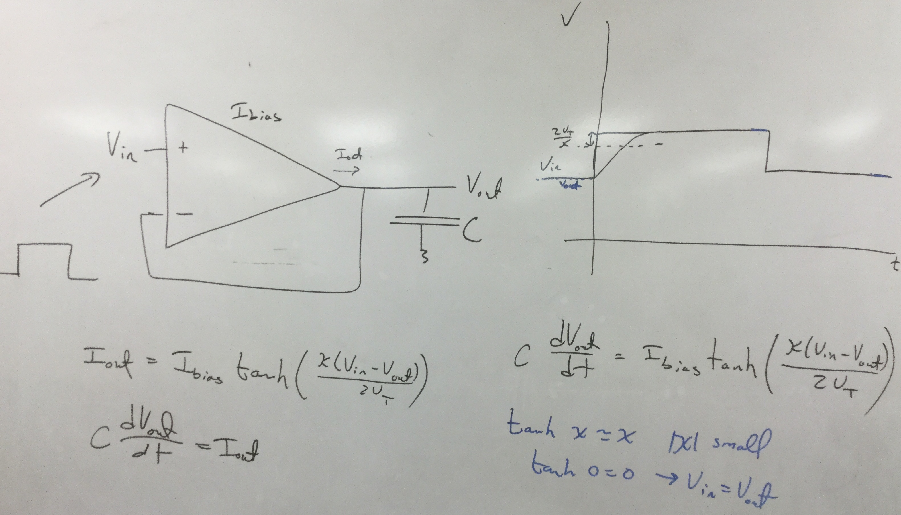
Trans-Bio Channels, Tuning TA FC I-mirror dynamics 1-T amp dynamics Dynamics Linear Analysis for TA LPF Exp Intro FPAA LPF Demo |
Transistor Channel Model. Follower-Integrator(Chp.9), Single-T Amps SubVT transfer functions | 1, 2, 3, 4, 5, 6, 7, 8, 9, |
Additional Reading / Watching
- Basic MOSFET characteristics: Subthreshold and Above Threshold
- Press on GT FPAA 2016 pdf
- Background information (if needed) on Drift & Diffusion Carrier Transport, on PN Junction Electrostatics to Band Diagram, and on PN Junction Band Diagrams.
- Interesting videos on machine Learning by CGP Grey and on Stealing Baseball Signs with a Phone
- Paper showing biological channel measured data from IEEE Midwest CAS 2023 (source)
FPAA Board and Tool Setup
Using the FPAA requires an Ubuntu Virtual Machine (VM) with our synthesis tools
- Ubuntu VM Download (scroll to the bottom)
- *Password = "Reverse"
Once downloaded the VM can be run using an emulation software such as Virtualbox . The USB service pack also needs to be downloaded to connect a laptop to the FPAA board.
To launch the FPAA tools off the VM, press the "CADSP" button on the left toolbar. Two screens will pop up, one for Scilab and one for the "Blue GUI." From here you can design and program circuits onto the FPAA.
To program a circuit onto the FPAA
- Start the VM and open the CADSP tools
- Connect the FPAA to your computer with a USB cable
- Confirm that the board is connected to your VM, and connect it manually if not
- Enter the corresponding board type and number into the blue GUI
- Choose the circuit you want to program through the blue GUI
- Hit "Compile Design"
- Hit "Program Design"
- Once programming finishes hit "Take Data"
- You can now measure your circuit!
- Keep properly grounded when handling FPAAs
- Only use one FPAA per group
- Never put > 2.5 or < 0 volts into the FPAA
- Documentation on setting up your system
- Helpful thoughts on FPAA System
- Documentation on extracting simulation data from Scilab
Experiment 1: MOSFET Transistor Modeling from Measurements
Static experimental measurements of MOSFET channel current versus gate voltage, source voltage, and drain voltage, both for nFET and pFET devices were taken off an FPAA.- nFET Gate sweep, Source sweep, and Drain sweep.
- pFET Gate sweep, Source sweep, and Drain sweep.
- Devices used 2.4V = Vdd.
- Drain: ~/rasp30/prog_assembly/libs/scilab_code/characterization/char_nFETpFET/Drain_nfet_sweep_(chip_number)_30a.csv
Gate Sweep
A gate sweep measurement is performed by measuring source current vs gate voltage, swept from GND to VDD. The source voltage is held at GND/VDD (nFET/pFET) to keep the device in saturation throughout the sweep.- Curve fit a line to the subthreshold region of the sweep.
- Extract kappa, threshold voltage, and Io
- Show a graph of log(Ids) vs Vg
- Show both experimental and curve fit data
- Identify any unexpected parts of the graph
Source Sweep
A source sweep measurement is performed by measuring source current vs source voltage, swept from GND to VDD. The drain voltage is held at GND/VDD (pFET/nFET). This data was taken at 300K.- Curve fit a line to the saturated portion of the curve (assume subthreshold)
- Extract UT
- Explain how the extracted UT compares with the expected value
Drain Sweep
A drain sweep measurement is performed by measuring source current vs drain voltage, swept from GND to VDD. The source voltage is held at GND/VDD (nFET/pFET), and the measurement is repeated for different gate voltages.- Plot the drain sweeps (log(Id) vs Vd) for different gate voltages
- Identify key regions (subthreshold, above threshold)
Transistor Simulation Model
The Scilab tools include simulation models for different components and systems, including transistors. Look at Examples/L2 Simulations/pFET or Examples/L2 Simulations/nFET for a starting simulation setup. Double click a component to open its parameters, which you can then change. Run a simualation by hitting Simulation/Start in the toolbar.
- Simulate gate, source, and drain sweeps
- Using your extracted parameters and a "sigma" = 0.005, try and match the experimental measurements
Writeup
In the lab report, please include at a minimum- Table of extracted parameters
- Gate sweep plot, including experimental data, curve fit, and simulation
- Source sweep plot, including experimental data, curve fit, and simulation
- Drain sweep plot, including experimental data and simulation
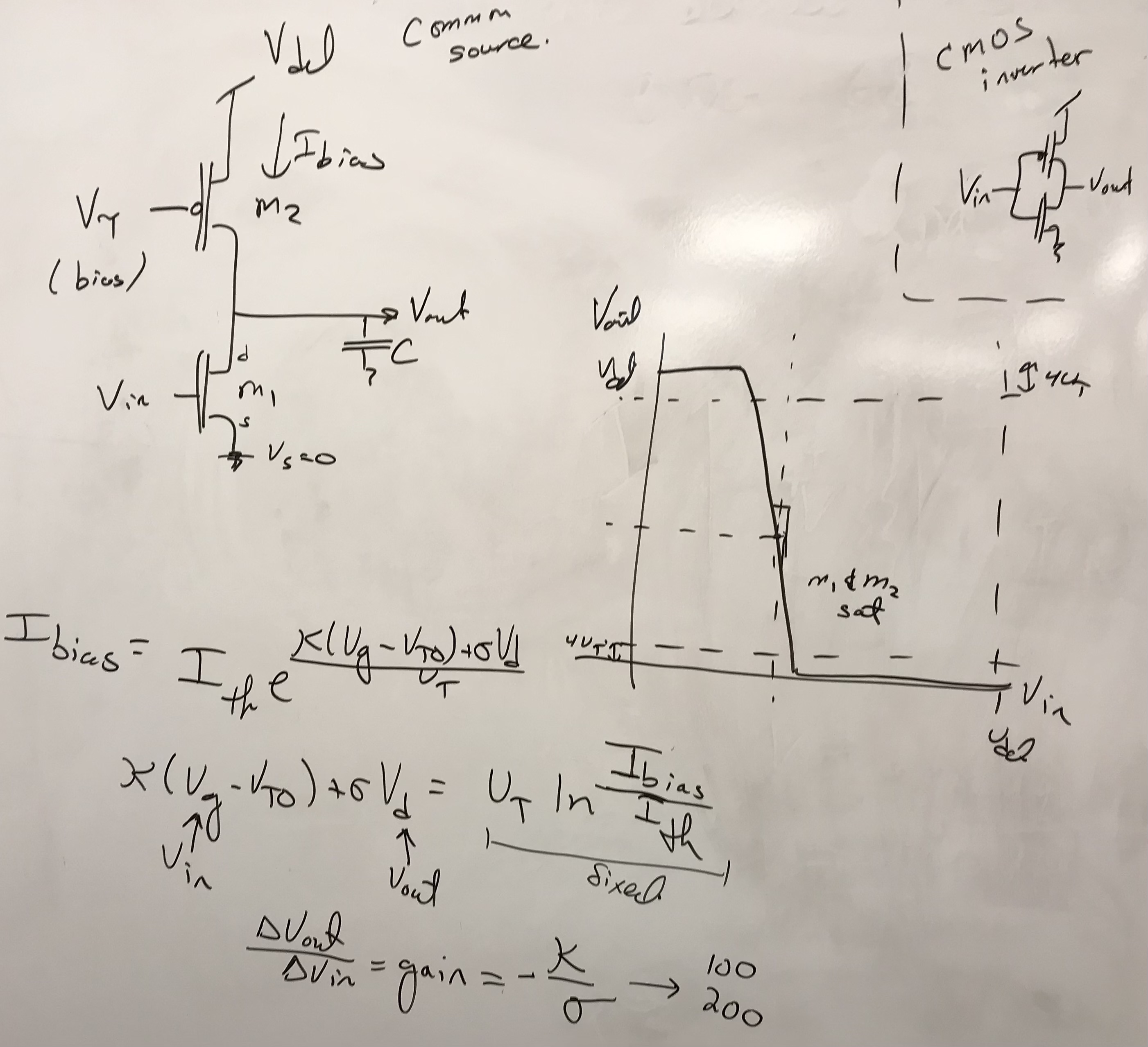
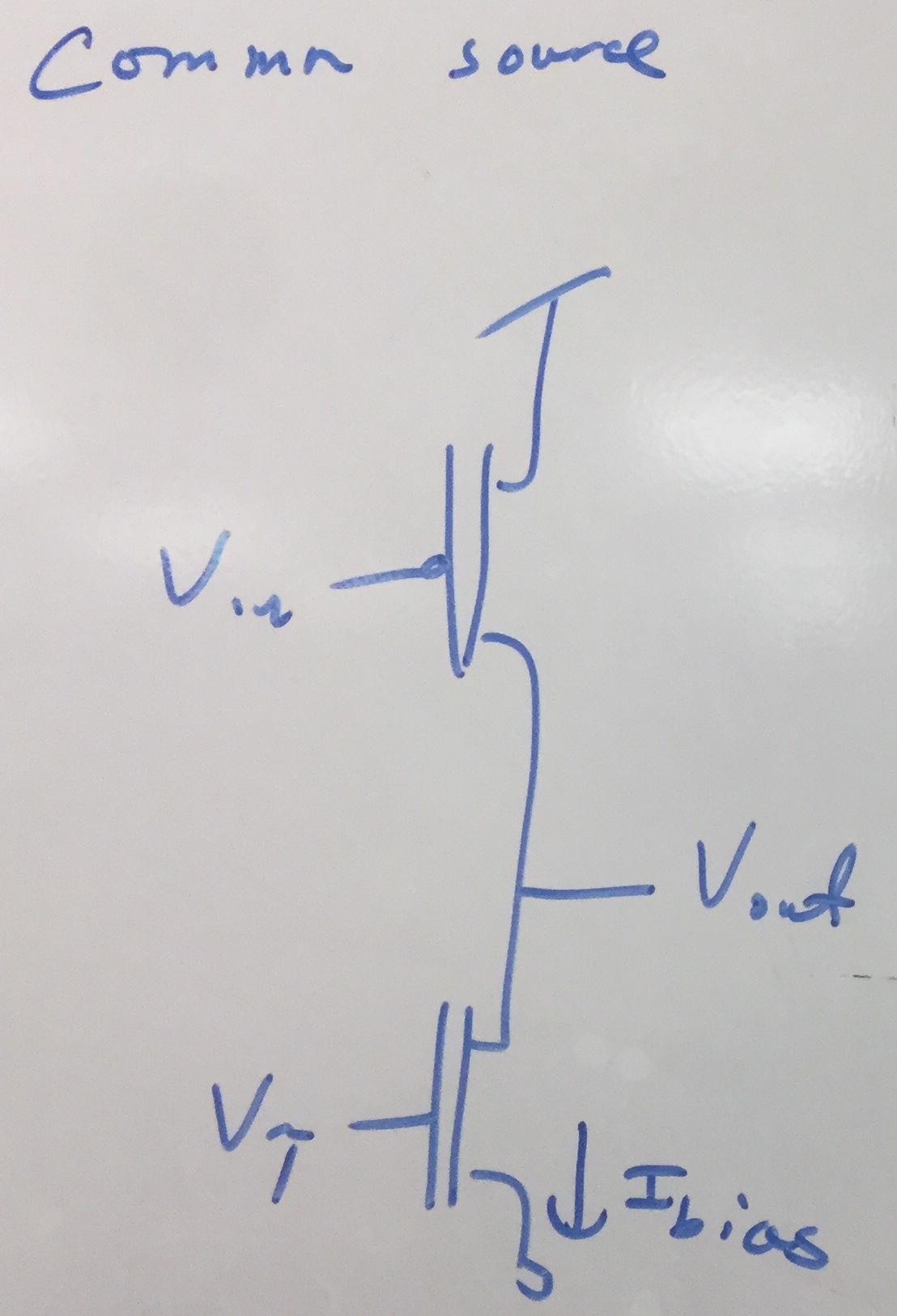
Experiment 2: Source Follower and Common-Source Amplifiers
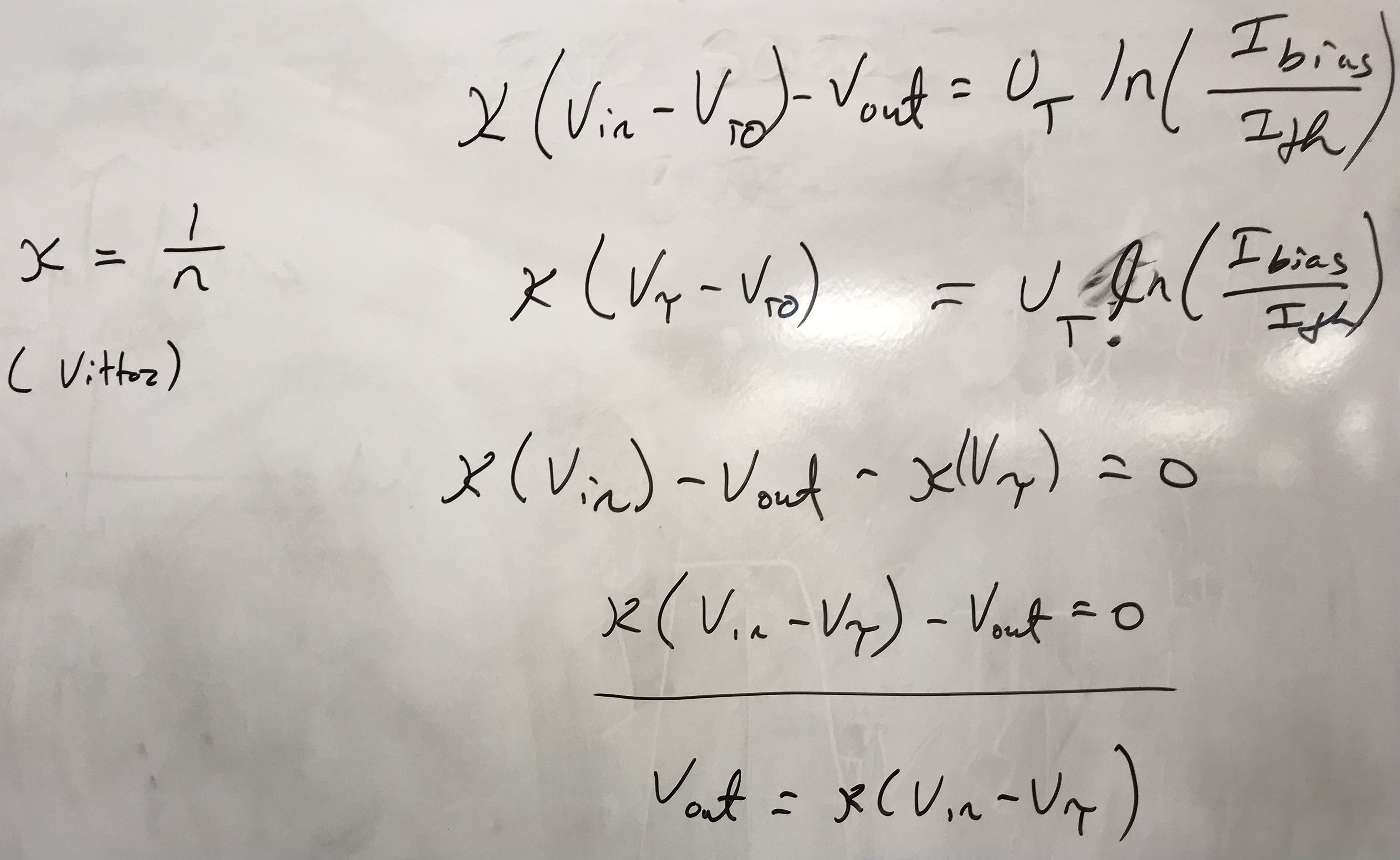
Single transistor amplifiers are basic building blocks behind more complex circuits. For both the source follower and common source amplifiers- Derive the transfer function in the gain region from large signal subthreshold EKV equations
- Compute the theoretical gain in this region
Source Follower Measurements
Program a Source Follower on the FPAA and simulate it using the tools.
- Measure Vin vs Vout for at least two values of Ibias
- Simulate Vin vs Vout for the same values of Ibias
- Compare the simulated and experimental measurements
- Curve fit the gain region
- Find gain
- Discuss why a source follower is a good measurement of how "kappa" changes for a fixed bias current
- Discuss how a change in "kappa" relates to depletion capacitance changes
Common-Source Measurements
Program a Common-Source amplifier onto the FPAA.
- Measure Vin vs Vout for a value of Ibias
- Curve fit the gain region
- Find gain
- Relate gain back to the derived transfer function, compare to measured parameters
- Estimate bias current level
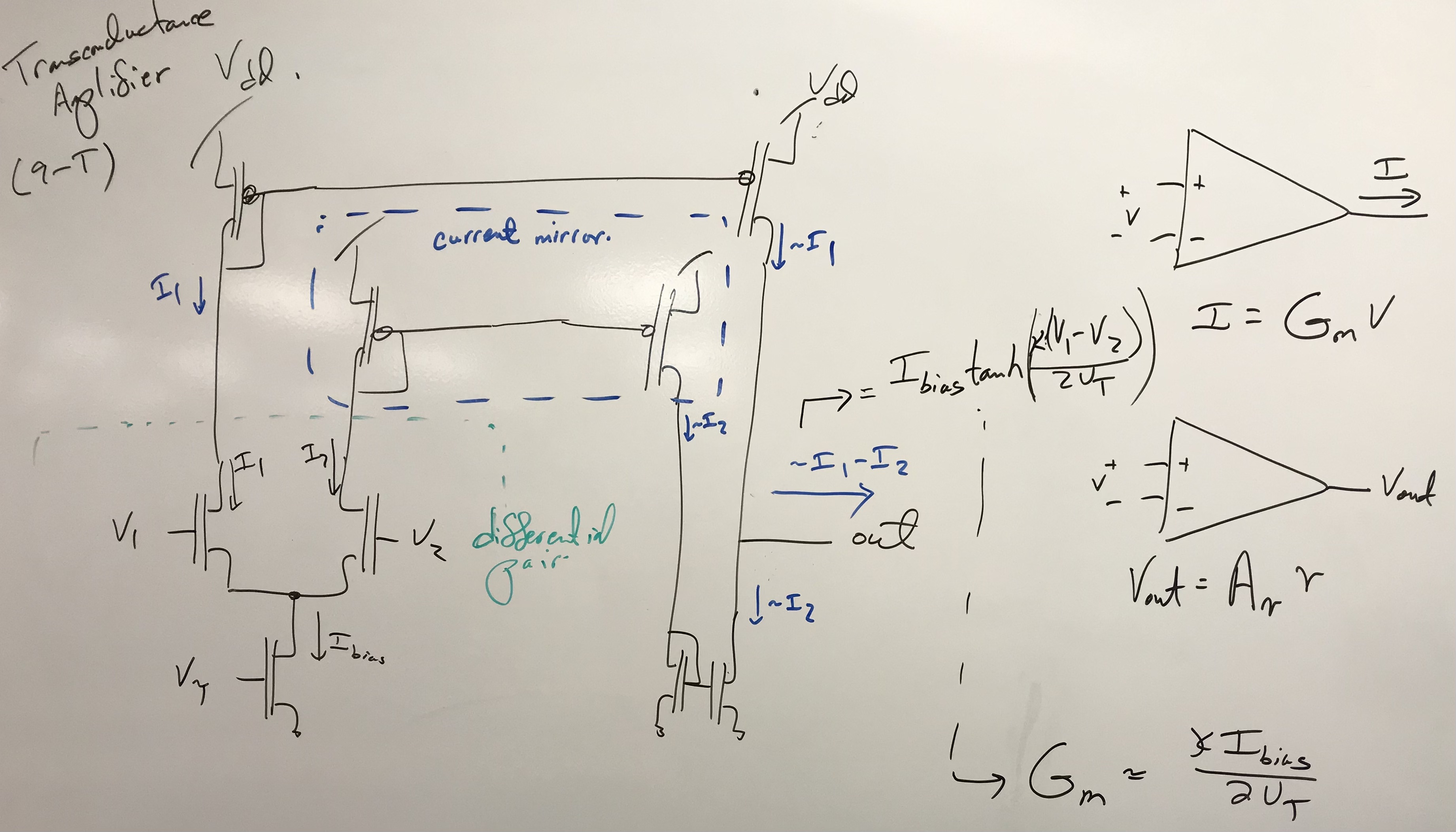
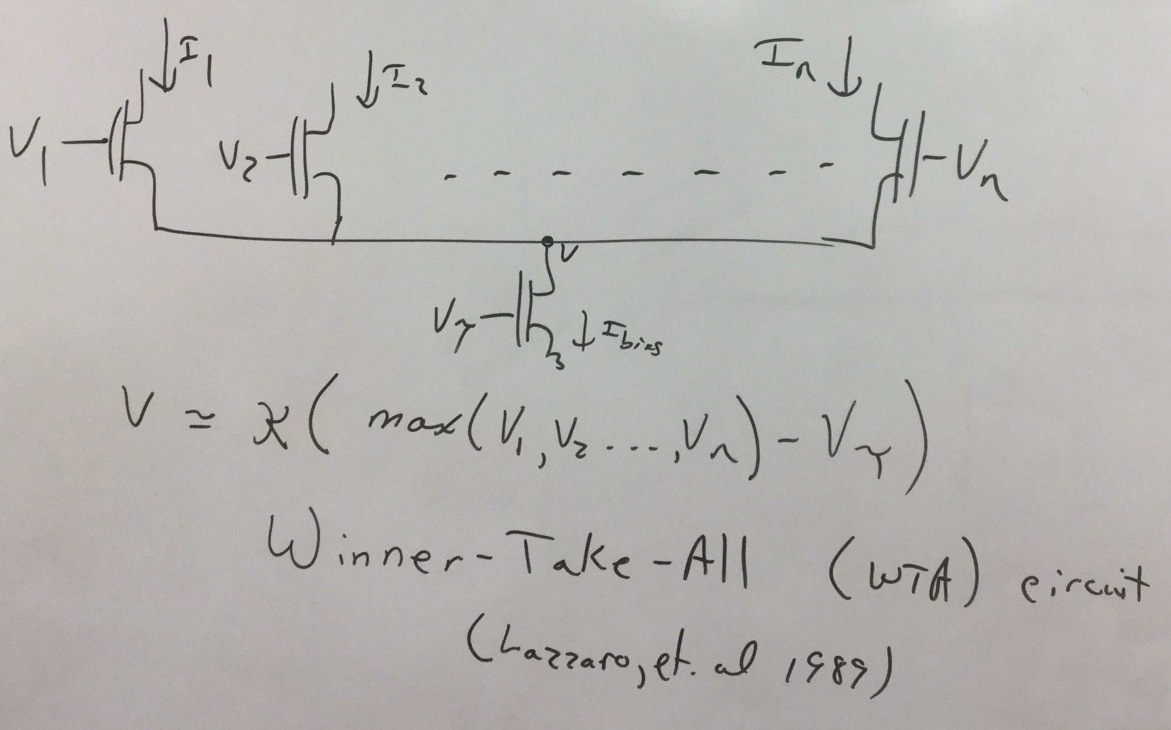
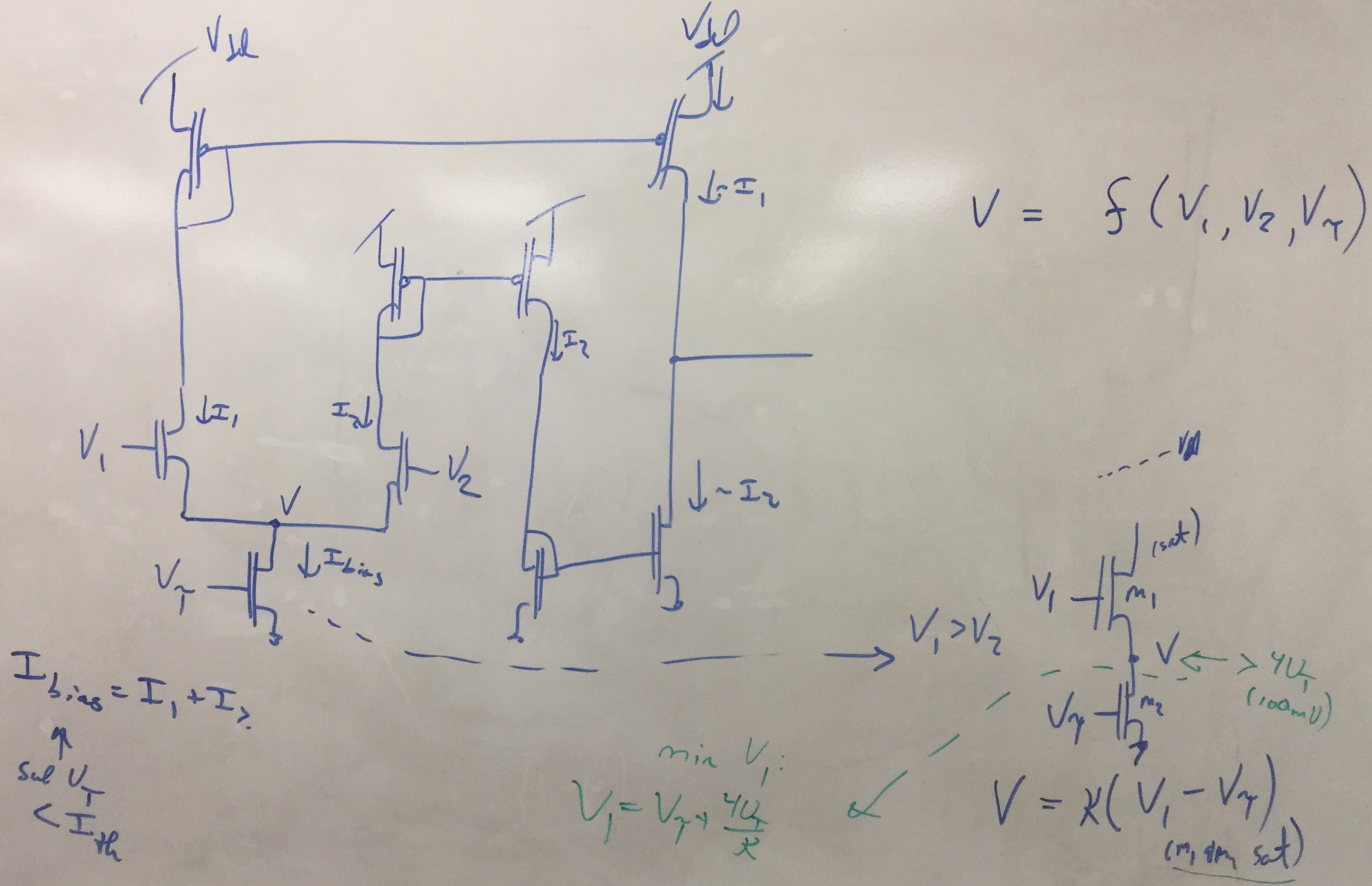
Experiment 3: 9T Transconductance Amplifier
A 9T Transconductance Amplifier (TA) exists as a basic component inside the FPAAs CABs. Each CAB contains two regular TAs and two Floating-Gate (FG) TAs. For a typical 9TA
- Derive the transfer function in the gain region from large signal subthreshold EKV equations
- Compute the theoretical gain in this region
Open Loop Configuration
Program a TA onto the FPAA with a bias current near the edge of subthreshold (100nA - 300nA). Fix one terminal at VDD/2 and use the other terminal as an input.
- Measure Vin vs Vout
- Curve fit the gain region
- Find gain
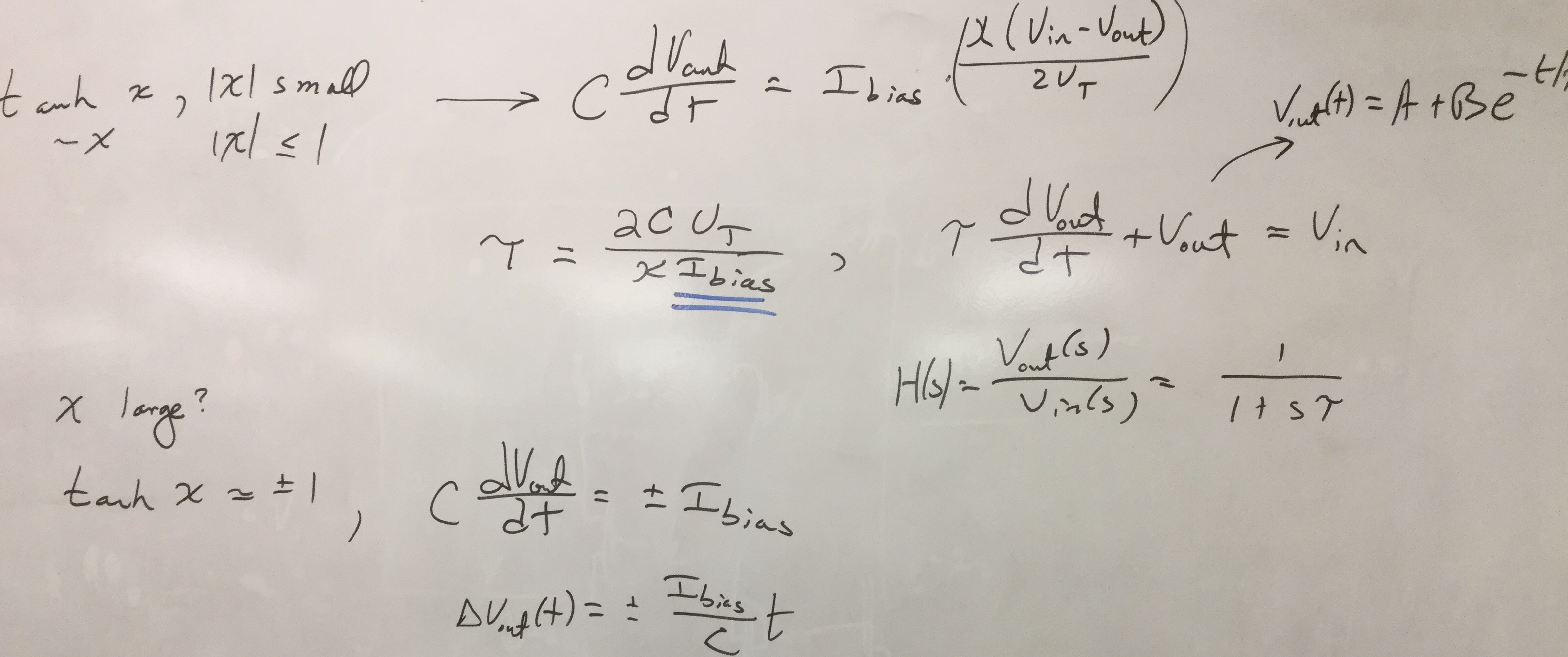
Voltage Follower/Buffer
Program a TA onto the FPAA at a low bias current (1 nA). Connect the negative terminal to the output (unity gain configuration) and use the positive terminal as an input.
- Measure Vin vs Vout
- Apply a small amplitude step (<40 mV pp) to Vin for two different bias currents
- Measure Vout and Vin vs time
- Apply a large amplitude step (>500 mV pp) to Vin for two different bias currents
- Measure Vout and Vin vs time
- Curve fit the linear region
- Find gain
- Explain what happens as the input approaches GND
- Curve fit the step responses to a linear RC behavior for both bias currents
- Determine the time constant of the circuit
- Is there a difference between rise and fall times?
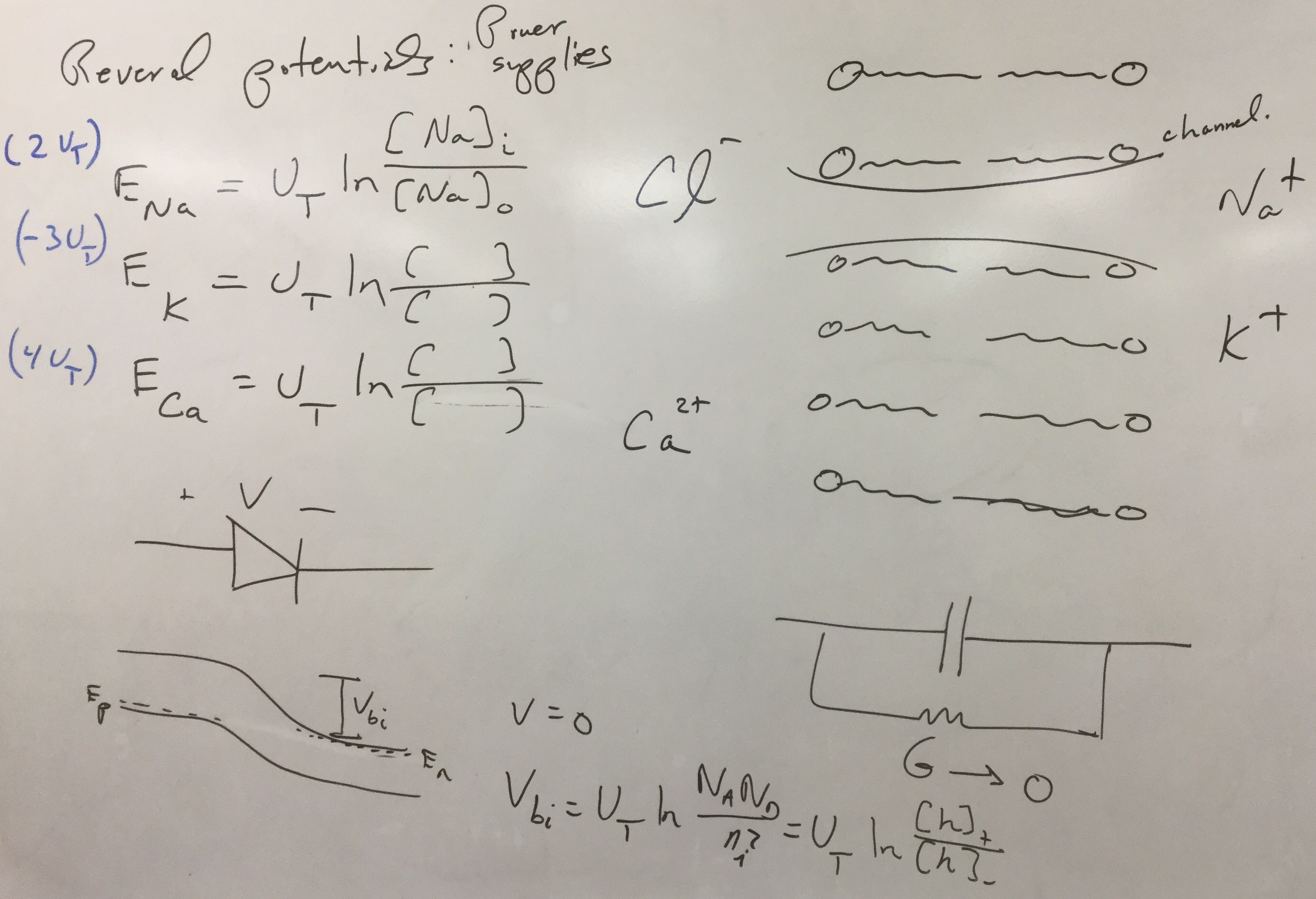
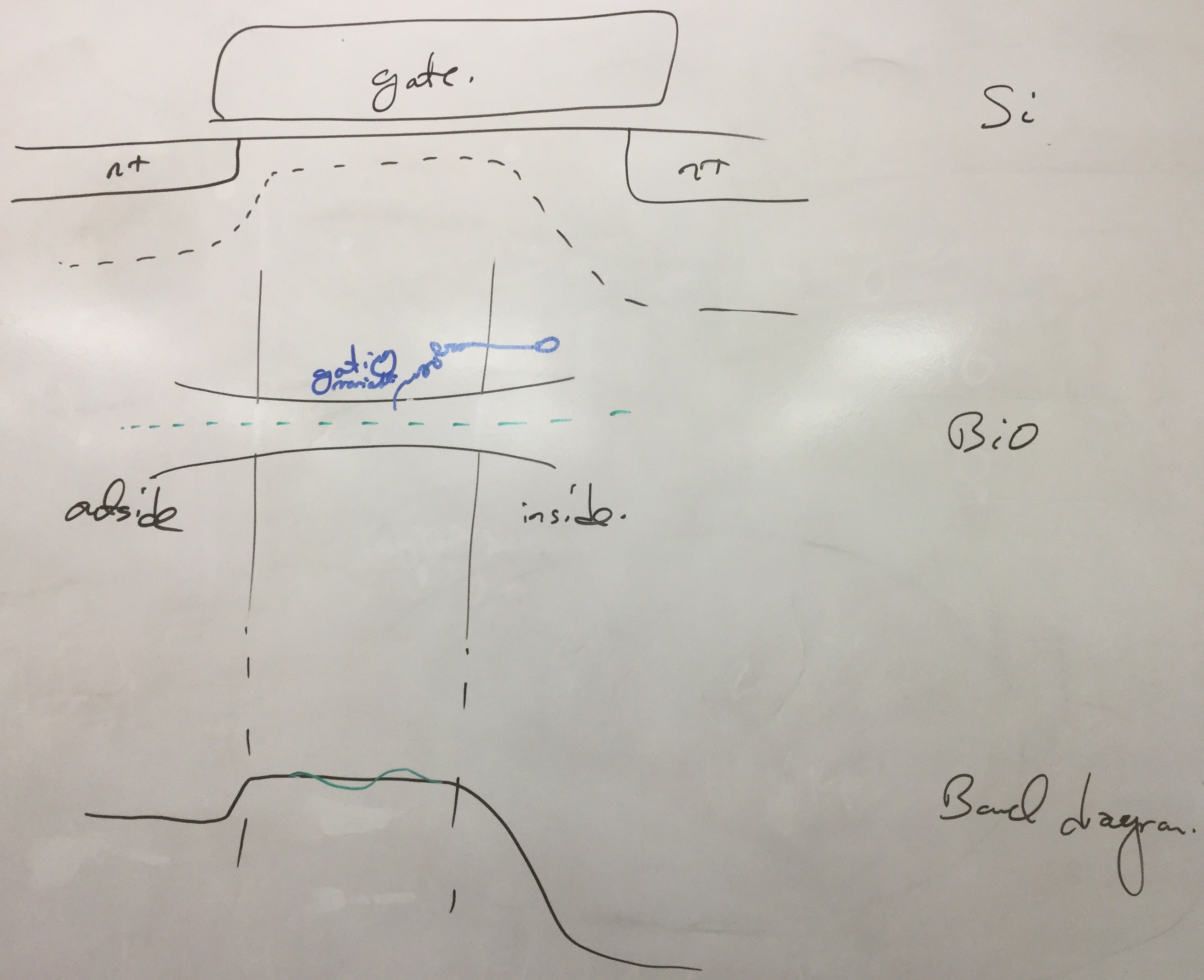
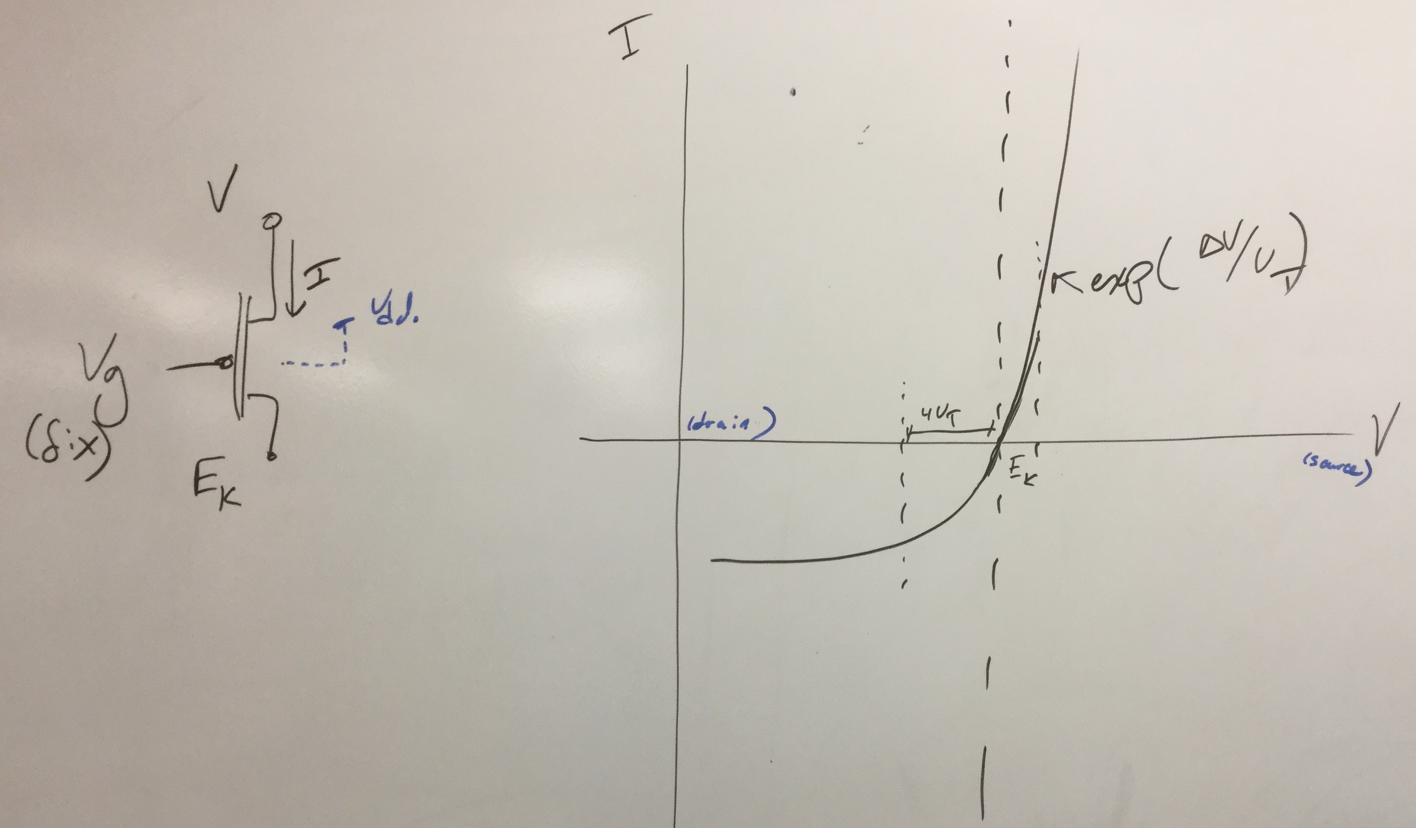
Passive Channel Transistor Model
The transistor is used as a silicon model for a biological passive channel. To test this we want to set up the transistor as a passive channel: the gate at a fixed potential, the source/drain at a fixed potential representing the voltage outside a cell, and the other voltage free to move representing the membrane voltage. For this setup
- Find a Current vs Membrane Voltage relationship
This measureent can be done in a few ways. If you have access to a picoammeter, simply measuring the current through the transistor and sweeping the membrane voltage will suffice. Without access to a picoammeter the measurement can be done in reverse: inject a current using a strong source such as a Transconductance Amplifier and measure the resulting output membrane voltage. You will want to do this for both current in and out of the transistor to account for the non-zero voltage outside the cell; take enough points to get the general shape of the curve.
Our model of a passive channel also has an associated capacitance with it (from parasitics).
- Using the small-signal response of a sudden input step, calculate the silicon membrane capacitance.
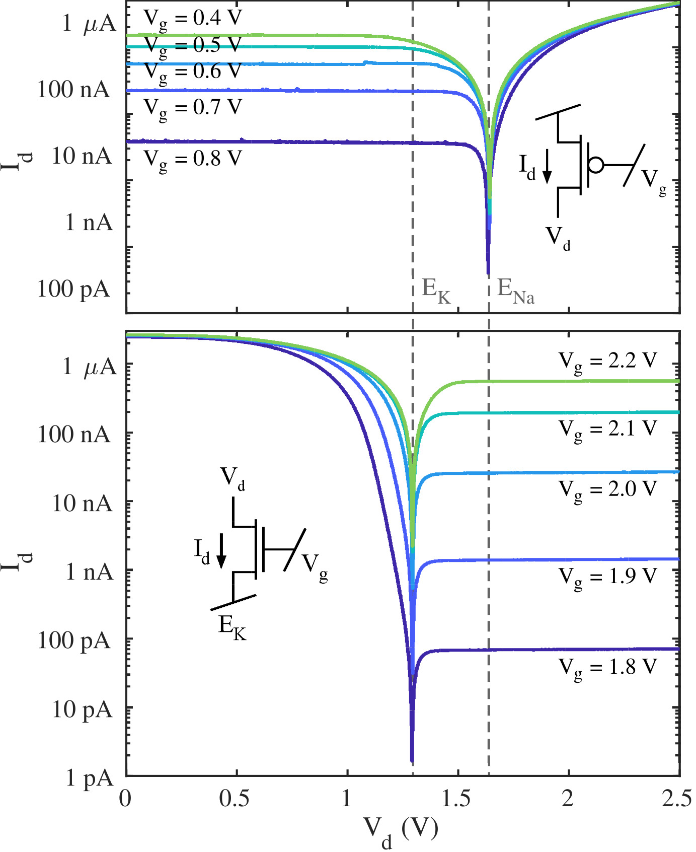
Reversal Potential: One might consider a biological system having GND, and yet, we need a higher potential, as all signals go between GND and Vdd. One might want to have the biological zero voltage as a mid-rail voltage (e.g. 1.35V).
Some additional comments:- If you are using external measurement equipment, please ensure the pins you are using are functional for their intended purpose (Input/Output), since previous classes may have damaged them. This can be tested by programming OTA buffers. Please note that on the documentation for the 3.0A board, the pinout after pin 14 is incorrect, and the output pins are every other pin (so pin 15 is 2 pins over from pin 14, and so on).
- If measuring using external devices, please ensure that you use raw/unbuffered output pins to avoid your curves clipping due to the output buffers. You might use a digital multimeter, or high-impedance (10x) probes if measuring with an oscilloscope. If you see a flatline output, try increasing the bias currents to ~100nA or changing CABs with fix location.
- For high-gain open-loop measurement, a more symmetric transfer curve can be obtained by holding the positive input fixed and sweeping the negative input. For high-gain measurements, it often important to do a course input voltage sweep, and then do a fine sweep where the high-gain changes happens. The number of points taken is important in measuring gain, and a gain that corresponds to measurements.