|
This unit is primary making the jump between analyzing transistors with the understanding they are
voltage-controlled current sources to
building core analog circuit from these devices
leading to basic amplifier design.

Topics
- MOSFET as an approximate current source
- Basic MOSFET Circuits: Common-Source, Common-Gate, Source Follower, Differential Pairs
- Transconductance Amplifiers (TA) / Basics of FG Circuits
Class Schedule and Video Viewing
|
Date
|
Class Topic
|
On-Line Lectures
|
Reading Material
|
White Boards
| |
Sept 12
|
Transistor Circuits
|
MOSFET = Current Source
One Transistor Circuit Basics
|
SubVT
transfer functions
| |
Sept 14
|
Transistor Amplifiers
|
Building Dependent Sources
High-Gain
Single-T
Amps
MOSFETCascode Circuit
|
|
1,
2,
3,
4,
5,
6,
7,
8,
9,
| |
Sept 19
|
Differential Pairs
|
FET Diff
Pair
Diff V
Amplifiers
Above-VT diff-pair
|
Chp. 5: Diff pair + TA
Chp. 6: More TA Circuits
|
1,
2,
3,
4,
5,
6,
7,
8,
| |
Sept 21
|
Dynamics
|
Tuning TA
FC
I-mirror dynamics
1-T amp dynamics
|
Chp. 9: Follower-Integrator
|
1,
2,
3,
4,
5,
| |
Sept 26
|
Small-Signal Model
|
Nonlinear TA
Dynamics
Small Signal FET Models
Linear Analysis for TA
|
|
1,
2,
3,
4,
5,
6,
| |
Sept 28
|
Noise
|
MOSFET noise
Source follower/ kT/C noise
|
Transistor
noise
|
1,
2,
3,
4,
5,
6,
| |
Oct 3
|
More Amplifiers
|
State Holding Divider
Capacitor-Focused Op-amp Circuit
C-R Op-Amp Example
|
Classic Amp Design
|
1,
2,
3,
4,
5,
6,
7
| |
Oct 5
|
Project Review
Virtual Class
|
|
|

Project Due Oct 6.
Reading Material
- Chapter 5 Material : OTA Circuit basics, Differential Transistor Pairs
- Chapter 6 Material : Cool Circuit Techniques
- Chapter 9 Material : Follower-Integrator Circuit
- Slide on subthreshold
transfer functions
-
Classic paper on Neural Amplifiers and Sub VT--Above VT
Design
-
Classic paper on transistor
noise
-
Initial paper (ISCAS 2018) on how analog design would be restructured
given a modular and programmable analog design style
(pdf).
The first figure likely will make more sense if
you have seen Monty Python's Holy Grail before.
Course Materials
Taped Lectures by Others
Lectures from Dr. Brad Minch (Olin) tht might be helpful:
-
CMOS
Inverter
Voltage Transfer Characteristic
-
CMOS Multiplexor Design and the Intrinsic
Gain
of MOS Transistors
-
Source Follower
Voltage Transfer Characteristics:
-
Cascode
Bias Voltage Generation
-
Qualitative MOS Differential
Pair
-
Weak Inversion
Operation of the MOS Differential Pair
-
Strong Inversion Operation of the MOS Differential Pair / Simple
5-T
Differential Amplifier
-
Common-Mode
Gain of the Simple MOS Differential Amplifier
-
Current-Mirror
Differential Amplifier Operation and Common-Mode Gain
-
Frequency
Response of the Current-Mirror Differential Amplifier
-
Frequency Response of the Current-Mirror Differential Amplifier:
Internal
Node Capacitances
-
MOS
Cascode
Configuration and the Mirror-Cascode Differential Amplifier
-
Frequency Response of the Mirror-Cascode Diff Amp /
Deciding Where to Account for the
Early
Effect
-
Layout design
of a Current-Mirror Differential Amplifier
Previous year Lecture Boards (2019)
- Starting of Dynamic Analysis:
1 ,
2 ,
- Dynamic Analysis and Small-Signal Modeling:
1 ,
2 ,
3 ,
4 ,
- Circuit Abstraction: Source Degeneration and Cascode Circuits:
1 ,
2 ,
3 ,
- Cascode and Folded Cascode Circuits:
1 ,
2 ,
- Transistor and Circuit Noise:
1 ,
2 ,
3 ,
4 ,
5 ,
6 ,
- Symmetric circuits: Common and Differential Mode:
1 ,
2 ,
- More Common Mode and Differential Mode Examples:
1 ,
2 ,
- Common-Source amplifier analysis sub VT and above VT:
1 ,
Previous year lecture boards (2017)
- Lecture 9 Boards:
1 ,
2 ,
3 ,
- Lecture 10 Boards:
1 ,
2 ,
3 ,
4 ,
5 ,
6 ,
- Lecture 11 Boards:
1 ,
2 ,
3 ,
4 ,
- Lecture 12 Boards:
1 ,
2 ,
3 ,
4 ,
5 ,
6 ,
- Lecture 13 Boards:
1 ,
2 ,
3 ,
4 ,
5 ,
- Lecture 14 Boards:
1 ,
2 ,
3 ,
4 ,
5 ,
- Lecture 15 Boards:
1 ,
2 ,
3 ,
4 ,
- Lecture 16 Boards:
1 ,
2 ,
3 ,
4 ,
- Lecture 17 Boards:
1 ,
2 ,
3 ,
4 ,
5 ,
- Lecture 19 Boards (exam solution lecture):
1 ,
2 ,
3 ,
4 ,
5 ,
Project Items
This project will leverage our measured results that we built our
EKV simulation model
in the last project
to look at MOSFET circuits, their IC design,
and the resulting issues in circuit design.
This project will look at
MOSFET transistor circuits,
in analysis, in simulation, and in IC layout.
This project will focus on
capacitors, particularly questions of MOSFET parasitics.
This project will consider
- source follower and common source amplifier.
- differential pairs and differential amplifiers.
- Initial understanding of bootstrap voltage / current reference.
This project will require the design of amplifier using a transconductance topology.
amd potential use of this amplifier.
In particular,
you will use a 9-transistor amplifier design and
add the appropriate cascode devices.
You will utilize the outputs of the bootstrap current source
to bias your amplifier.
Please remember
"kappa" does not equal 1 anywhere in this project.
You have transistor values from your previous project,
and you should use them, assuming you had correct values.
If you do not have confidence in your values,
you have access to the other projects for correct values.
I do not need a detailed derivation in the writeup,
just 1-2 highlights. Most derivations can be done effectively by inspection
with the right intuition.
For the particular bias currents required, you might need to have biases or inputs
that are outside the power supplies (below GND or above Vdd).
This should only be effectively necessary for the
common-drain and common source amplifiers.
Other cases should happen as part of the circuit.
This occurs because of the low-current biases that you are trying to
achieve with the low VT0.
Another way to achieve this case is taking your source terminal
up from GND (or down from Vdd),
which would happen in practical circuits.
For this project, you will want to use the following capacitances for your
capacitance modeling:
Cox = 10.4fF/ um2,
Col = 0.1fF / um,
n+ diffusion (0 bias) area capacitance to substrate:
Cj0n = 0.8fF/ um2,
n+ diffusion (0 bias) perimeter capacitance to substrate:
Cjswn = 0.034fF / um,
p+ diffusion (0 bias) area capacitance to substrate:
Cj0p = 1.05fF/ um2,
p+ diffusion (0 bias) perimeter capacitance to substrate:
Cjswn = 0.047fF / um,
Analyzing Bootstrap Current Source
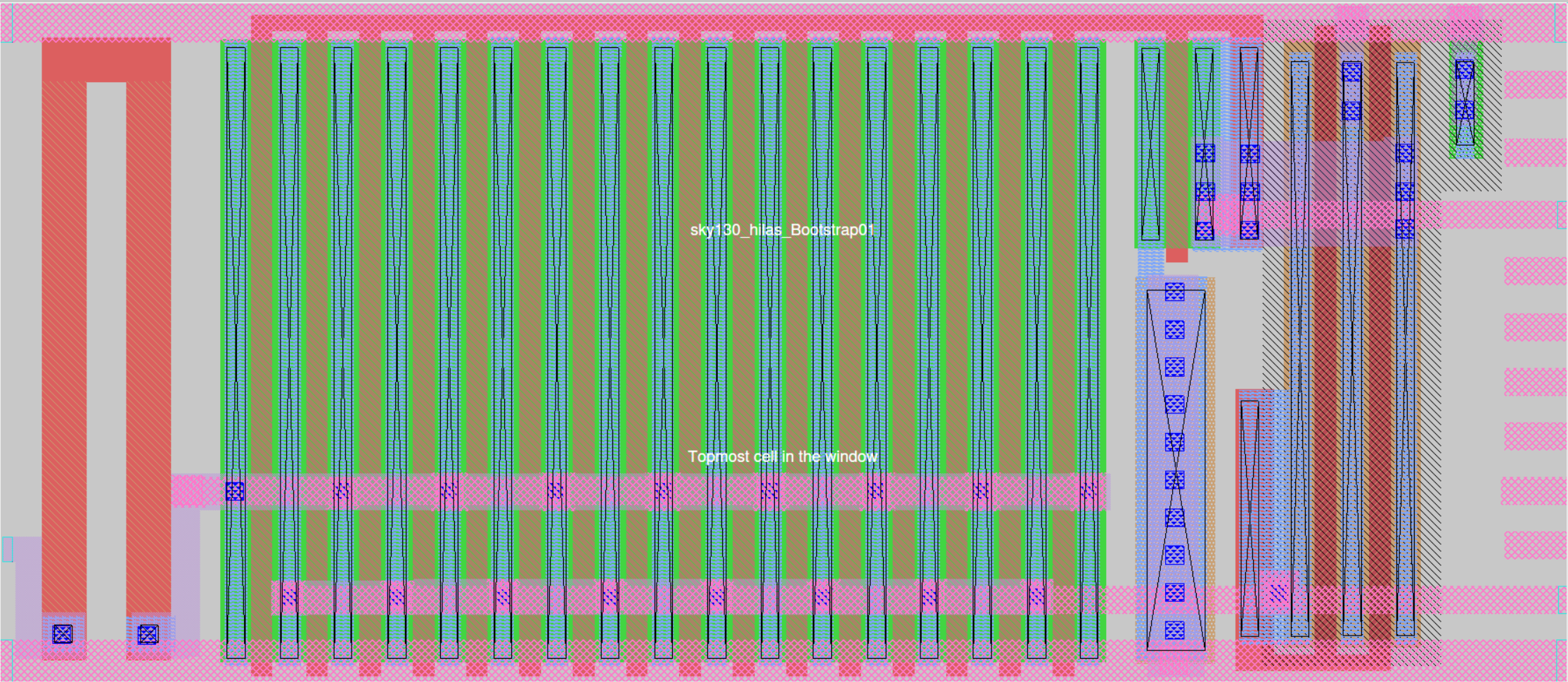
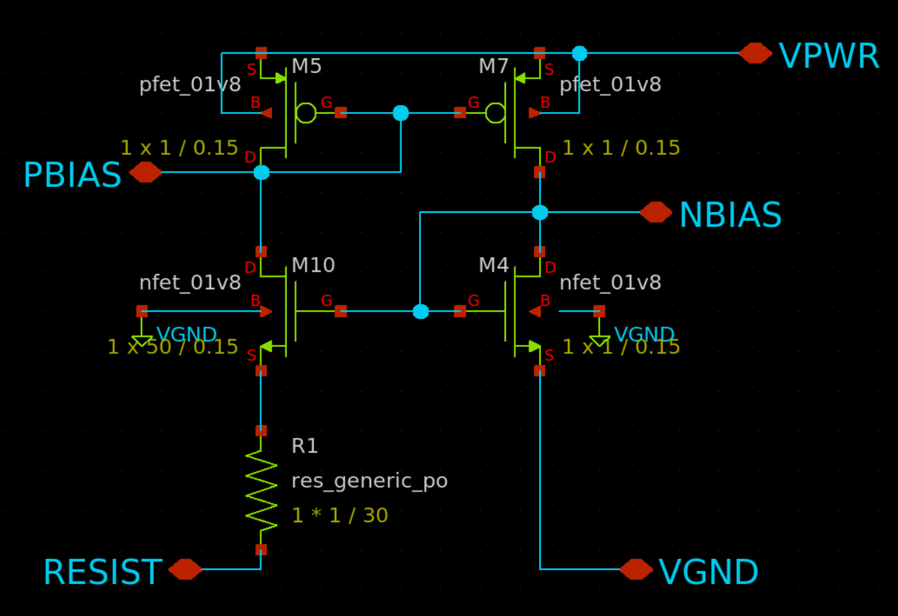
The bias structure for your circuits is the following bootstrap current / voltage reference.
Your circuits will work within this framework, and therefore you need to be able to analyze
the voltages for this particular bootstrap circuit as it is given in layout.
Assume the layout of the structure would be given for your design for this project.
The schematic does not have the proper W/L values or resistor values.
You should find those values.
The resistor value is the minimum resistance value;
often RESIST will be brought out to a pin and one can add addtional resistance.
You should be able to have a schematic that would LVS with the resulting circuit.
The bootstrap current source (without its startup circuit):
magic,
Xschem.
Labels are power supply (VPWR, 1.8V) and gnd (VGND),
a connection to add more resistance (RESIST),
and the resulting two output pins (PBIAS, NBIAS).
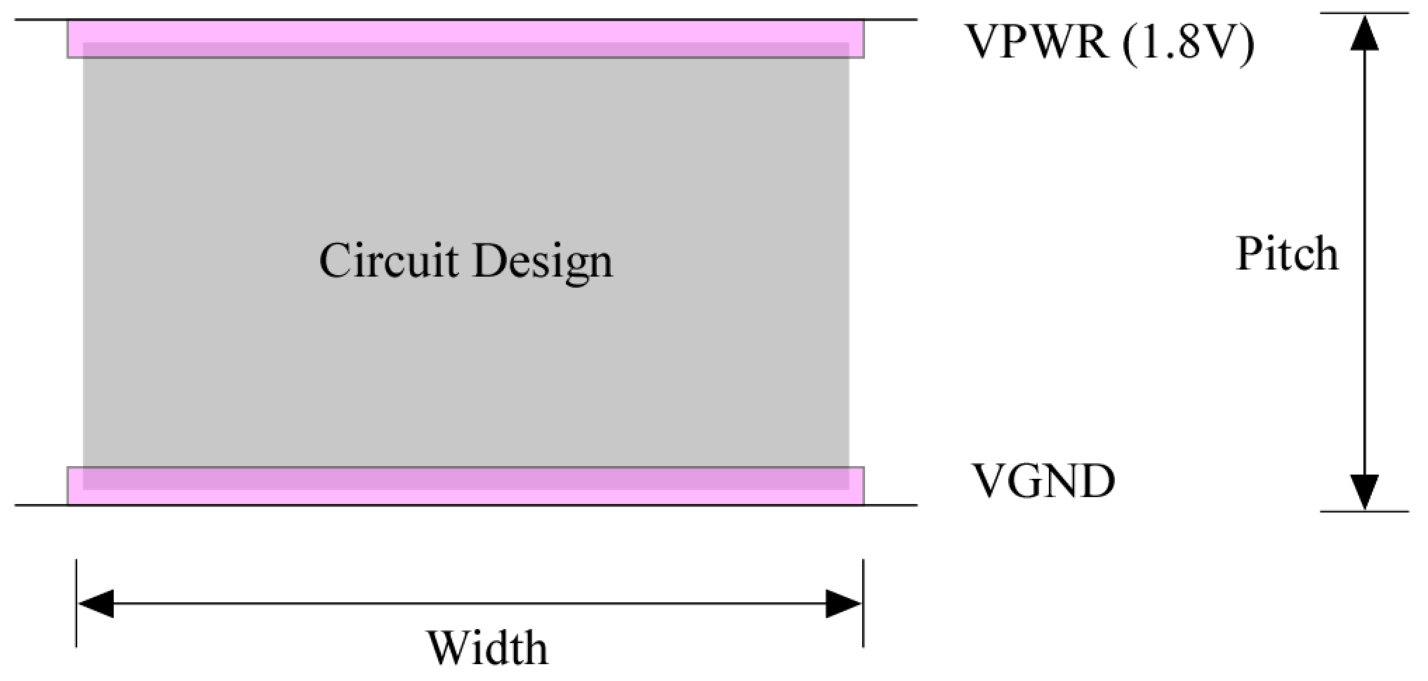
Your layout for this semester will be fitting into a standard size and framework,
where your design will have a constant pitch and your two supplies will be at the edge of the design.
The pitch, or vertical dimension for this Skywater 130nm CMOS process is 6500nm.
The width is a part of your particular design.

|
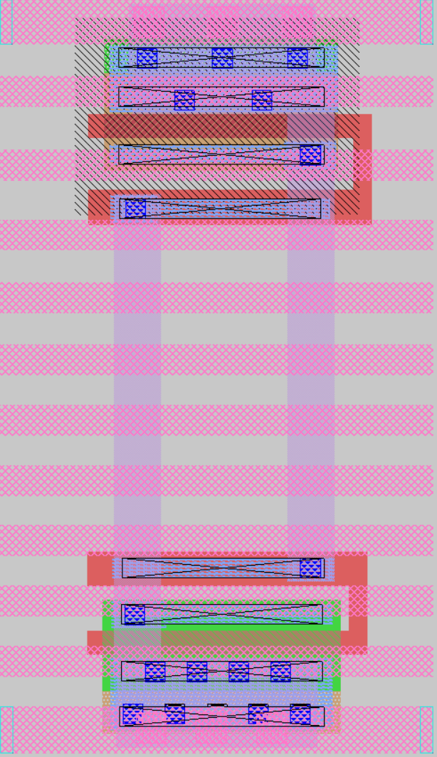
The spacer cell might help further understanding of the cell definition:
magic.
|

|
Questions:
- For the layout given, what is the value of the resistor in the layout
/ what is the ohms / square for the polysilicon layer?
What are the transistor W/L values?
What is Ith for each transistor?
Modify vaues of the Xschem for this block.
- What is the largest bias current for this circuit? (RESIST = VGND).
- Simulate (DC) this resulting structure for the bias current
using the given resistor
as well as for a added external 100kOhm resistor.
- How much does the bias current change for a change in the power supply
(VPWR = Vdd) = 1.8V)?
More specifically, if the supply changed by 100mV,
what is the change in the bias current
and output voltages?
- If there is a threshold-voltage mismatch on the transistors of 10mV,
how would that change the resulting reference response?
For the rest of the project, assume your reference has a 100kOhm resistor at VPWR to GND.
Two-Transistor Amplifiers
For each of these circuits,
-
Transistors for this part require W/L = 800nm / 400nm (Drawn values).
- You should have a load capacitance of 100fF.
In your simulation, just use a single capacitor of this size.
- Set gate voltage (from the bias structure)
for the bias transistor such that the bias current would be 10nA.
Identify that particular voltage.
Source-Follower Circuits
You need to make a source-follower circuit where the input signal goes
into a pFET gate.
You need to layout the source-follower circuit that must fit in the 6500nm pitch.
Include a picture of the layout (that agrees through LVS),
and use your layout to extract for your simulation file.
Analysis :
For your source-follower circuit:
-
What is the voltage gain from input to output?
How does the gain change from subthreshold to above-threshold bias currents?
Where is the gain region of the circuit?
-
From your (simulation) data and analysis of the source follower,
you can find kappa as a function of source voltage.
It turns out this configuration is a good measurement
of how kappa changes for a fixed bias current.
Compute a numerical derivative of the data and discuss your results.
Discuss how this change in "kappa" would be related to changes in depletion capacitance.
- What is the corner frequency of this circuit for the bias current listed above?
What is the linear range of this circuit?
- What is the total noise (output) of this circuit?
How does total noise (output) of this circuit change with subthreshold bias currents?
Qualitatively, how does it change for above threshold bias currents?
Simulation :
For your source-follower circuit:
-
Simulate a transfer curve for your Source-Follower circuit.
Identify the operating regime for the amplifier circuit,
that is, the place where both transistor are operating in saturation.
Identify the slope of the amplifier in this region,
and compare the value to your analytic results.
- Simulate the amplifier with a upgoing and downgoing step response
(a square wave).
Use two step amplitudes,
one smaller than the amplifier's linear range and
one larger than the amplifier's linear range.
Curve fit for the time constant and the linear range of the amplifier
for both signals.
Which parasitics made the biggest difference between your theory and simulation?
-
In practice, the source follower will not have constant gain because of kappa shift.
Does the simulation show this change? What do you get for kappa versus output voltage?
Need numerical derivative.
- What is the total measured output noise (thermal) of this circuit?
Common-Source Circuits
You need to make a common-source circuit where the input signal goes
into an nFET gate.
You need to layout the common-source amplifer within the 6500nm pitch,
include a picture of the layout (that agrees through LVS),
and use your layout to extract for your simulation file.
Analysis :
For your common-source circuit:
-
What is the voltage gain from input to output?
Where is the gain region of the circuit?
-
How does this gain depend upon bias current in subthreshold?
Quantitatively explain how the gain changes for above threshold current levels.
- If you needed a very high gain amplifier of this type,
how would your design your transistors to achieve this very large gain?
- What is the corner frequency of this circuit for the bias current listed above?
What is the linear range of this circuit?
- What is the total noise (output) of this circuit?
How does total noise (output) of this circuit change with subthreshold bias currents?
Qualitatively, how does it change for above threshold bias currents?
Simulation :
For your common-source circuit: (bias current = 10nA)
-
Simulate a transfer curve for your Common-Source circuit.
You will likely want a sweep over the operating range to find the gain region.
Then,
obtain a dense sweep of the transfer curve between the amplifier (gate) input and the amplifier output (drain). Notice where the data makes a sharp transition, and relate this value to measured parameters and bias voltages.
Find the gain,
and compare to your values of Early Voltage (sigma), kappa, and UT.
- Make a single plot of the output voltage versus the input voltage for this amplifier.
Curve fit the gain of the amplifier
Identify the operating regime for the amplifier circuit,
that is, the place where both transistor are operating in saturation.
Identify the slope of the amplifier in this region,
and compare the value to your analytic results.
- Simulate the amplifier with a upgoing and downgoing step response
(a square wave).
Use a step amplitude such that both transistors are in saturation for the
entire response,
that is, you are in the high-gain region of the amplifier.
Curve fit for the time constant of the amplifier.
Which parasitics made the biggest difference between your theory and simulation?
- What is the total measured output noise (thermal) of this circuit?
Differential Pairs and Amplifiers
For each of these circuits,
-
Transistors for this part require W/L = 800nm / 400nm (Drawn values).
- You should have a load capacitance of 250fF.
In your simulation, just use a single capacitor of this size.
- Set gate voltage (from the bootstrap reference circuit)
for the bias transistor such that the bias current would be 10nA (a subthreshold current).
Differential Pairs :
Start by creating your layout (within 6500 pitch)
of your differential pair with an nFET current source
bias transistor.
Consider the following questions:
- Assume that the biasing current source transistor for a differential pair
is operating with subthreshold currents.
Explain if one can assume the differential pair devices are in subthreshold?
-
What is the minimum drain-to-source voltage required for this biasing current source transistor if it is operating with subthreshold currents?
- Derive the differential-pair output currents
as a function of the two differenital input voltages
and the bias current, assuming all transistors operate sub threshold.
You should neglect the effect of Early voltage (channel length) for this calculation.
- If V1 << V2, simplify the above expressions for I1 and I2. You will find this expression helpful for some of the experimental curve fits.
- Simulate for
currents versus differential input voltage.
Currents versus common-mode input voltage. How much does it change?
How does it relate to sigma / Early effect?
Differential Amplifiers :
Start by creating your layout of your 9 Transistor amplifier (within 6500nm pitch)
using the differential pair you built above.
Continue to use the same 10nA bias current.
Consider the following questions:
- Simulate the transfer curve response for your amplifier keeping the negative
input terminal fixed between the power supply rails (say half of Vdd).
What you need to do is do a voltage sweep on the inputs, keeping one input fixed,
and measure the output response.
You might need to do a course sweep and then a fine sweep to get the gain region.
Identify key regions of the graph.
- Connect your amplifier as a unity-gain amplifier.
We call a follower--integrator circuit (follower for low frequency operation).
Perform a transfer curve for this amplifier
(a sweep of the output voltage versus input voltage ).
Does anything unexpected happen as the input voltage approaches GND? Make a plot (linear scale) of Vout vs. Vin, with a curve fit over the linear region.
Is the gain exactly equal to 1?
Discuss how this result is a function of differential mode and common-mode gain.
-
Input a square wave input (like the above experiments)
where one input is smaller than the input linear range,
and one input is larger than the input linear range.
Analytically calculate your expected timeconstants.
What do you expect your linear range would be?
Extract the timeconstant and linear range from these step responses.
Determine the time constant of the integrator by curve fitting for your timeconstant
(removing steady state, looking at log of the remaining abs of the response).
What is the load capacitance?
Is there any difference between the rise and fall times?
Curve fit response to linear response (exp( -t / tau) ) to determine the time constant of the integrator in both cases,
as well as the linear range, where applicable.
What parasitics changed your values from your theoretically expected results?
Transconductance, Output Resistance, and Gain:
This part will quantitatively show the relationship between transconductance,
output resistance, and voltage gain for your amplifier circuit.
Again, you will use a 1nA bias current,
and will use the amplifier in its open-loop configuration.
-
Explain how you would measure the voltage gain for a transconductance amplifier if you were given
an ammeter and variable voltage source.
How will you compute the output resistance, Rout, and transconductance, Gm, from experimental measurementsr?
- From your previous simulations,
calculate what the transconductance would be for this amplifier
in its linear region.
Transconductance is asking what is the change in output current for a change in input voltage.
- From your transfer function,
calculate the gain of this amplifier in its gain region
(all transistors in saturation).
- Perform a large-signal sweep of output terminal current (input)
versus output terminal voltage.
Note where transistors are in saturation and when not in saturation.
In the linear region for the graph,
calculate the resulting output resistance.
- compare your three results. Do they agree, and how close do they agree?
Amplifier Design project
Using a transconductance amplifier topology,
your group is required to design the device
to typical on-chip operational amplifier specifications.
Each group will have a different specfication (Unity-gain frequency).
-
The design must have layout, LVS, extraction, and post-extraction simulation.
You have one amplifier design that you will perform the resulting post-layout simulation tasks.
You have full control over the W/L of all devices.
Most W/L won't have a major effect on your design.
-
Your layout must be in a vertical pitch of 6500nm.
If your layout does not fit in that space,
as well as it can be arrayed,
then your design is immediately not valid.
-
Your design area must be minimized, as well as rules must be followed.
You must identify the width (orthogonal dimension from vertical pitch) for your design.
-
Your group must submit your .mag file for your design;
as two individuals are working on a project,
the individual not uploading the report should upload their .mag design.
The file should have the two names of those submitting the design in your filename.
-
The gain of your amplifier is required to be 10,000.
You would expect to need cascode devices at the output node.
-
Capacitive load = 1pF. You can add more as required.
-
Your bias current needs to be minimized for your given specifications,
as well as justified for your given frequency response.
Your bias current voltage biases will be set through the bootstrap current source.
-
The input range for this amplifier must be valid
(specifications must hold) for voltages between 0 and 1V.
The output voltages need to be valid between 0.3V and 1.5V.
Vdd = 1.8V for this design.
-
Your group must comment on the impact of
transistor mismatch (e.g. cascode voltage, input offset).
Two nearby 400nm/200nm transistors will have roughly 10mV VT0 mismatch.
Your analysis requires having a discussion of transistor mismatch effects on your circuits.
Total thermal output noise is 1mV rms when the amplifier is
connected in its unity-gain configuration
(note: total noise (mV rms) as compared to
noise per unit bandwidth (mV rms / rt Hz) ).
The value would be equivalent to its total input referred noise.
Discus the noise per root Hz, and the resulting relationship required.
Your power consumption is limited to 3 times your
differential amplifier bias current from Vdd to GND
(differential amplifier for your TA, not from an earlier question).
Unity-Gain frequency will be given to each group.
You should measure the slew rate of your amplifier,
and relate it to your bias current,
as well as relate it to your unity-gain frequency.
Need to have 45 degree phase margin.
For this design, this phase margin requires the output capacitance be greater
than the total parasitic capacitances to fixed potentials for this circuit,
and you should make sure you satisfy this constraint.
You might need to add capacitance at the output to guarrentee this result.
Or you might be able to shift your transistor sizes to minimize some capacitances.
Tentitive rubric: I include a tentitive
rubric
that I am planning to use,
although I reserve the right to change any and all of it
for grading this project.
Additional Thoughts
- A tool that some might find interesting and
has a chance of being useful is the
Analog Designer's Toolbox
ADT
I do not endorse this tool or discourage this tool.
It might be helpful, and I certainly welcome any thoughts.
There is a Youtube overview
video ,
and they have a few other Youtube videos that might be interesting, including on
the gm/ID Design
Methodology .
|


