The goal of this project is to put the CMOS designs that we are learning in class to build a design for a CMOS Op Amp. Power supplies of 0V and 2.5V will power the circuit as the rest of the FPAA device.
The Op-Amp design must be compiled in the FPAA device. Simulation results can be very useful in combination with experimental results. Use of remote and physical hardware are both acceptable to reach the target metrics.
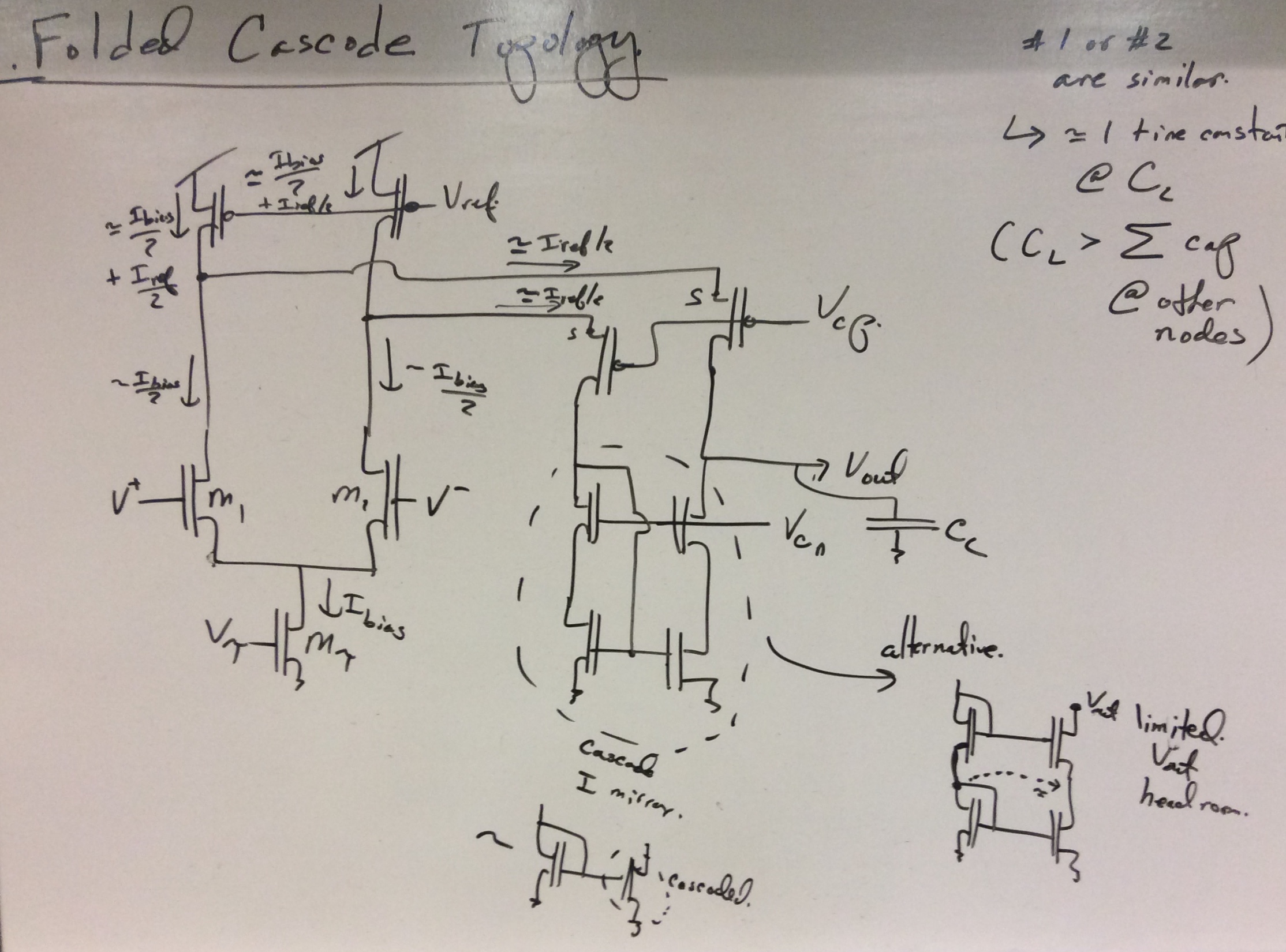
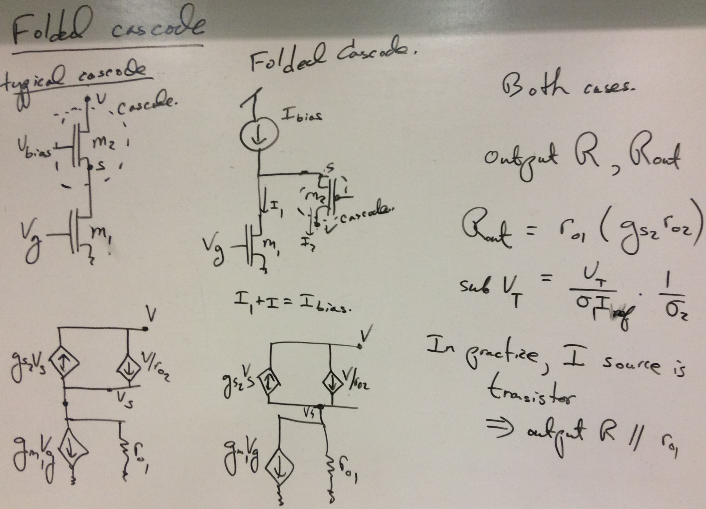
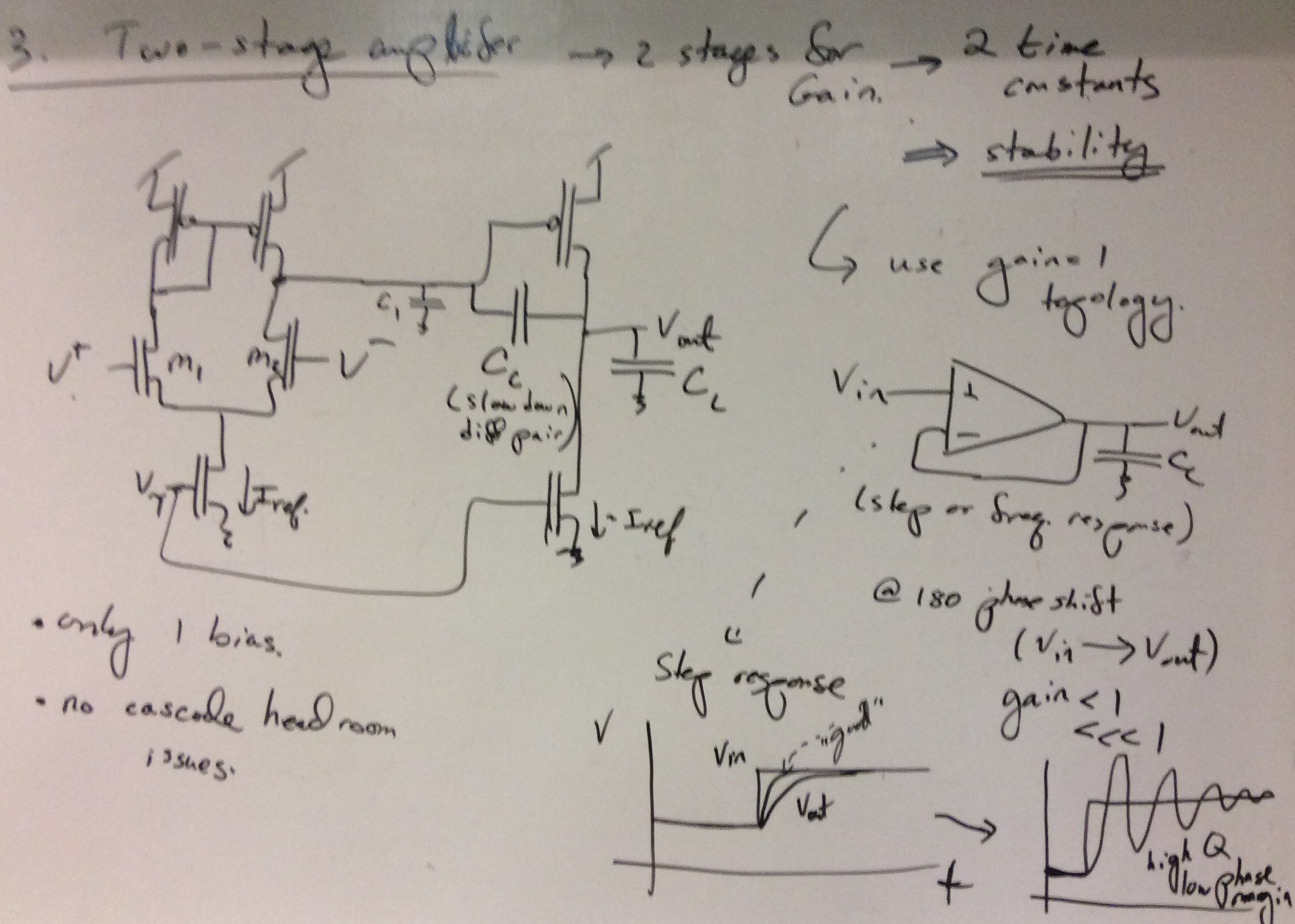
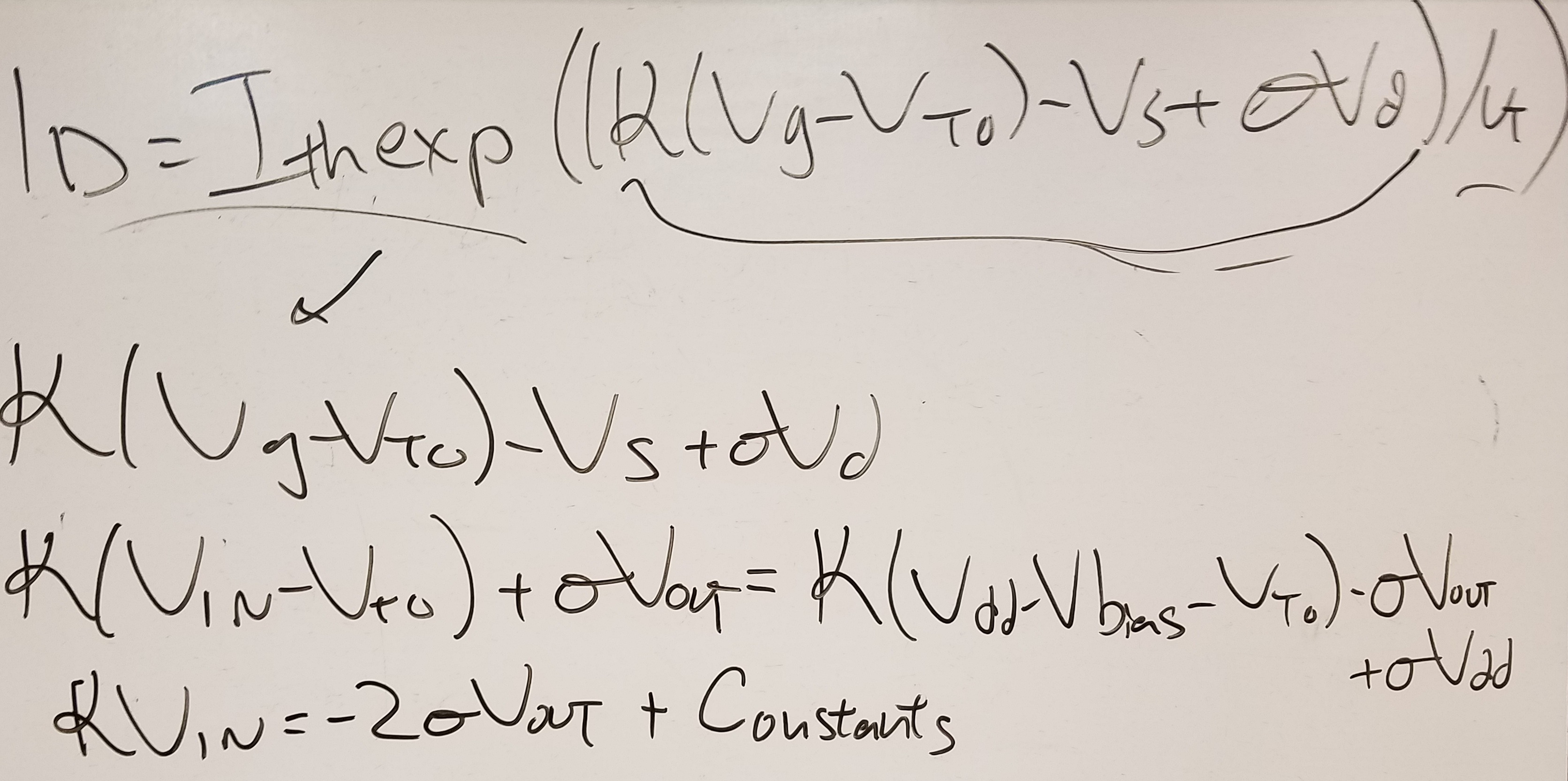
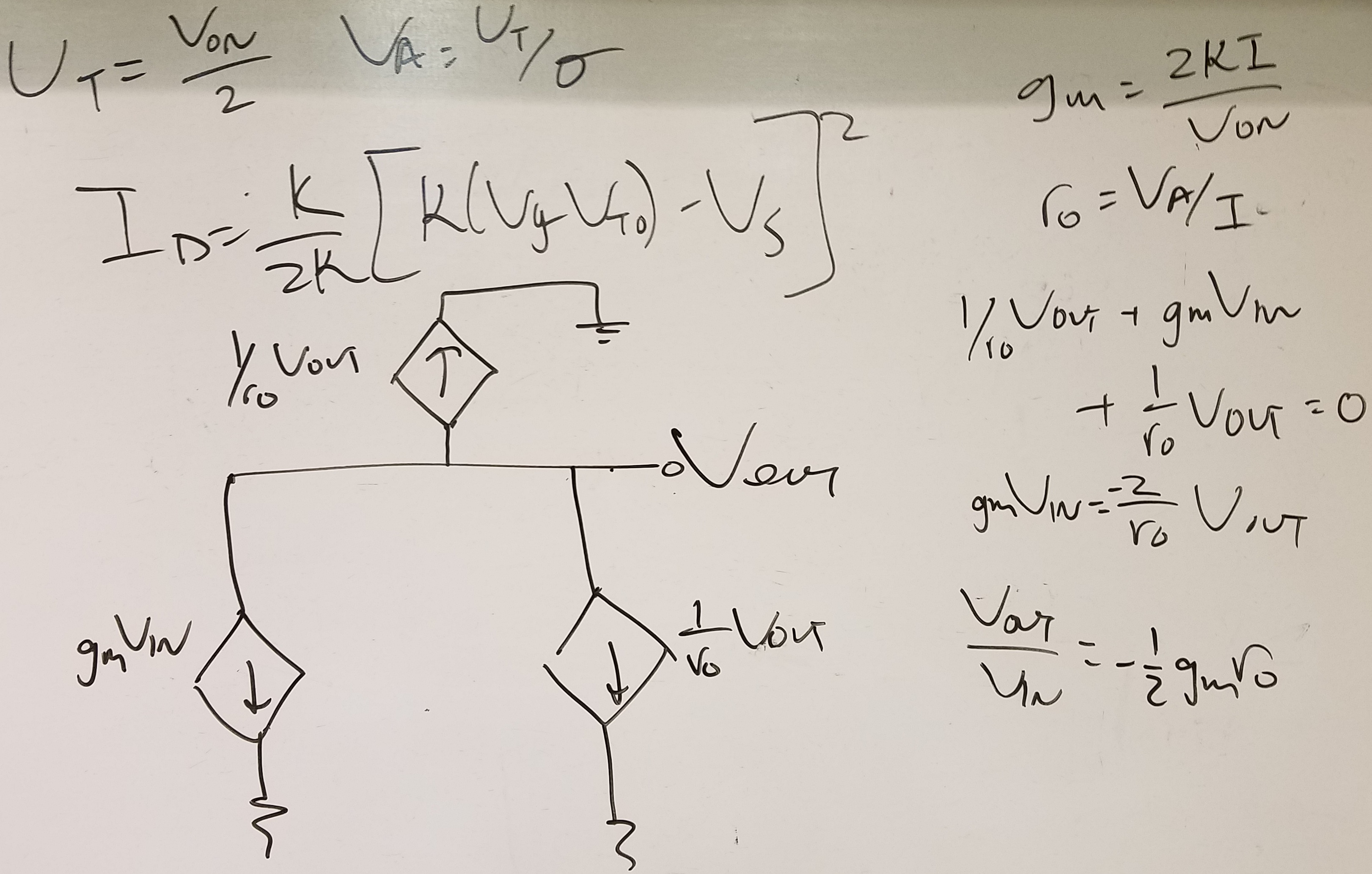
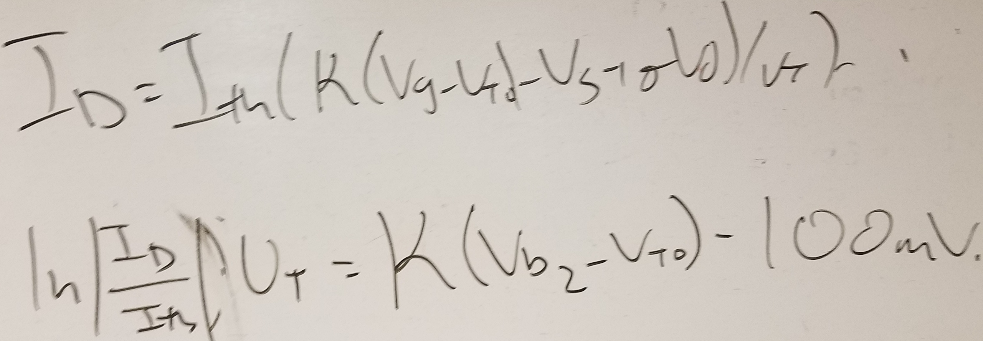
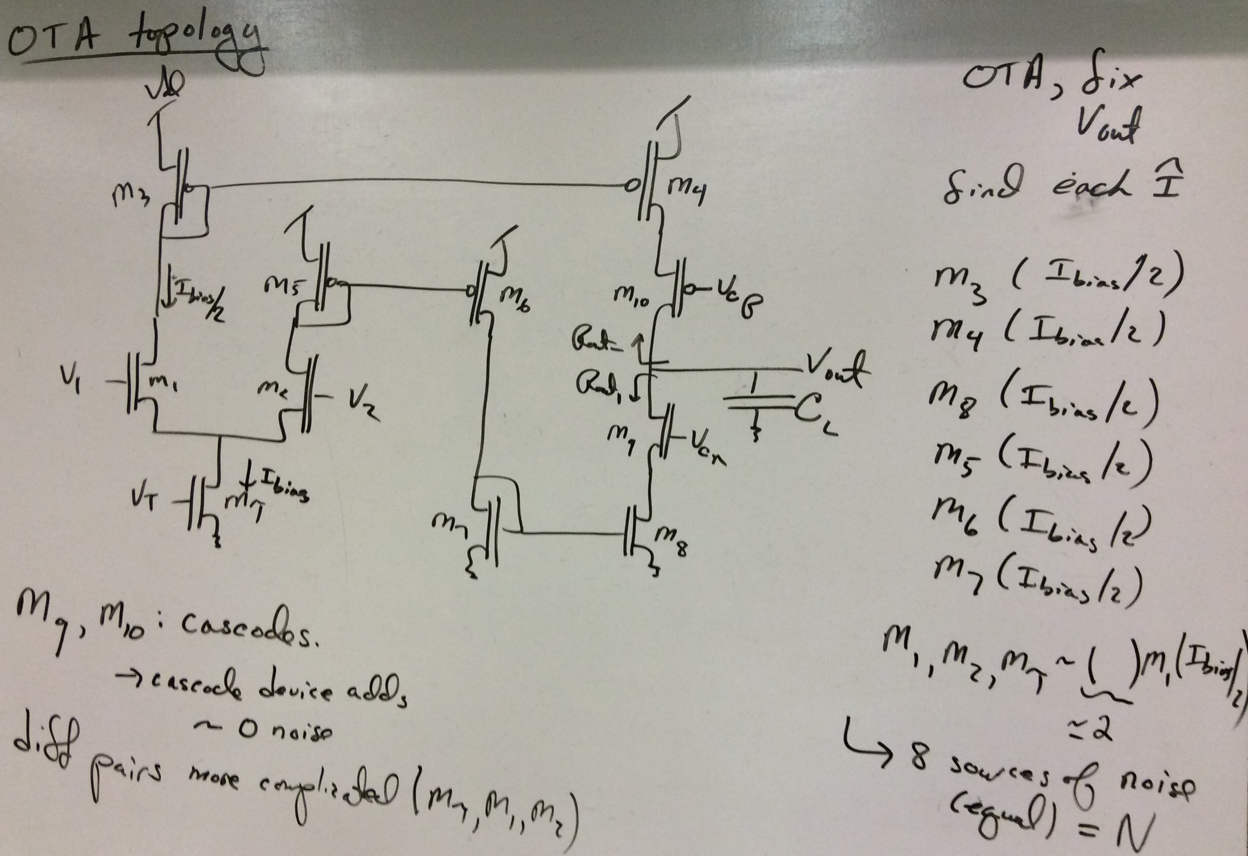
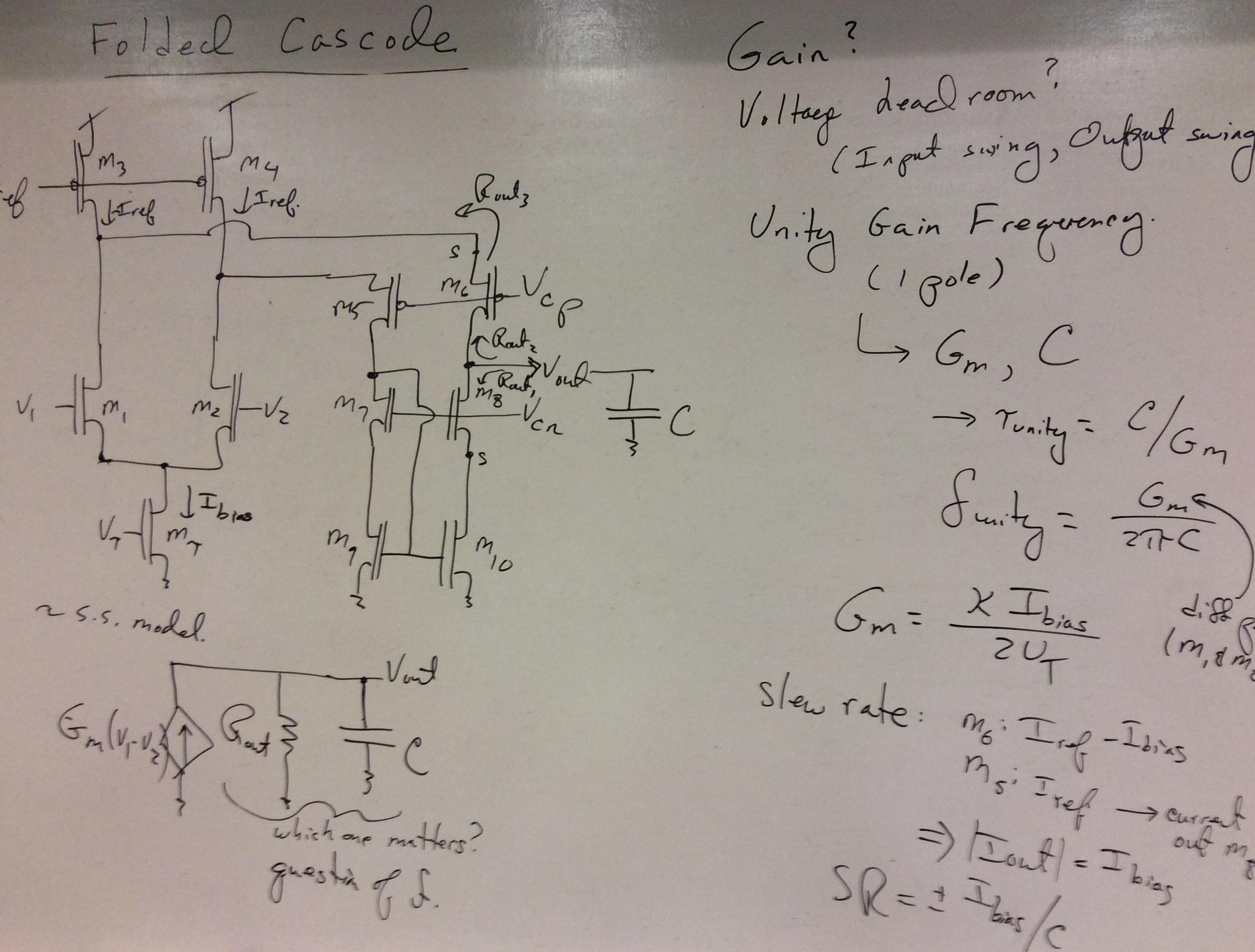
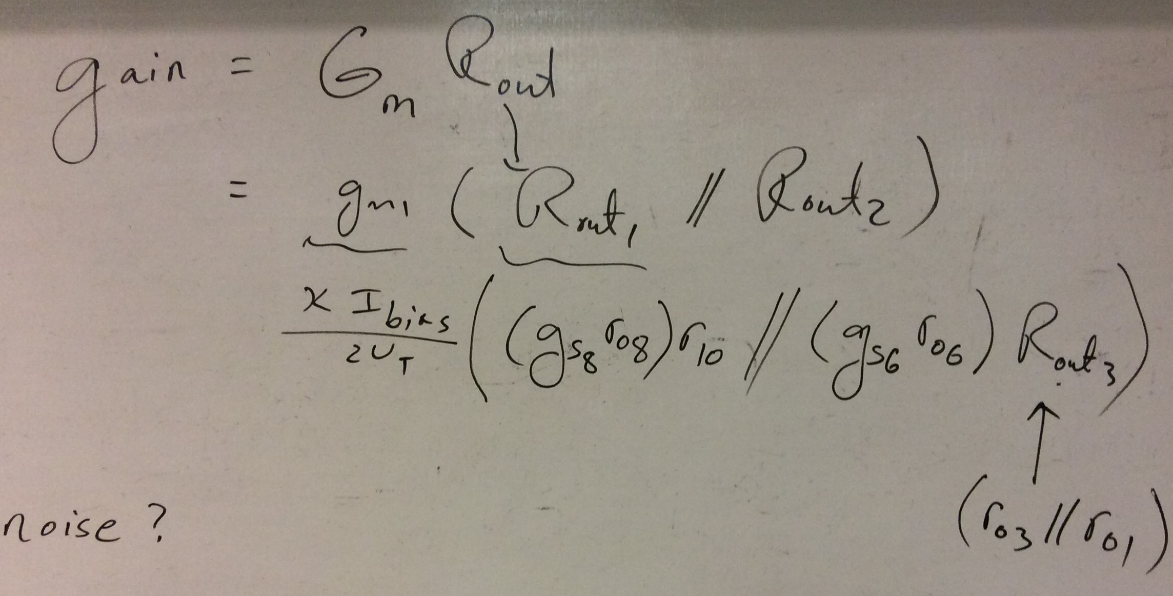
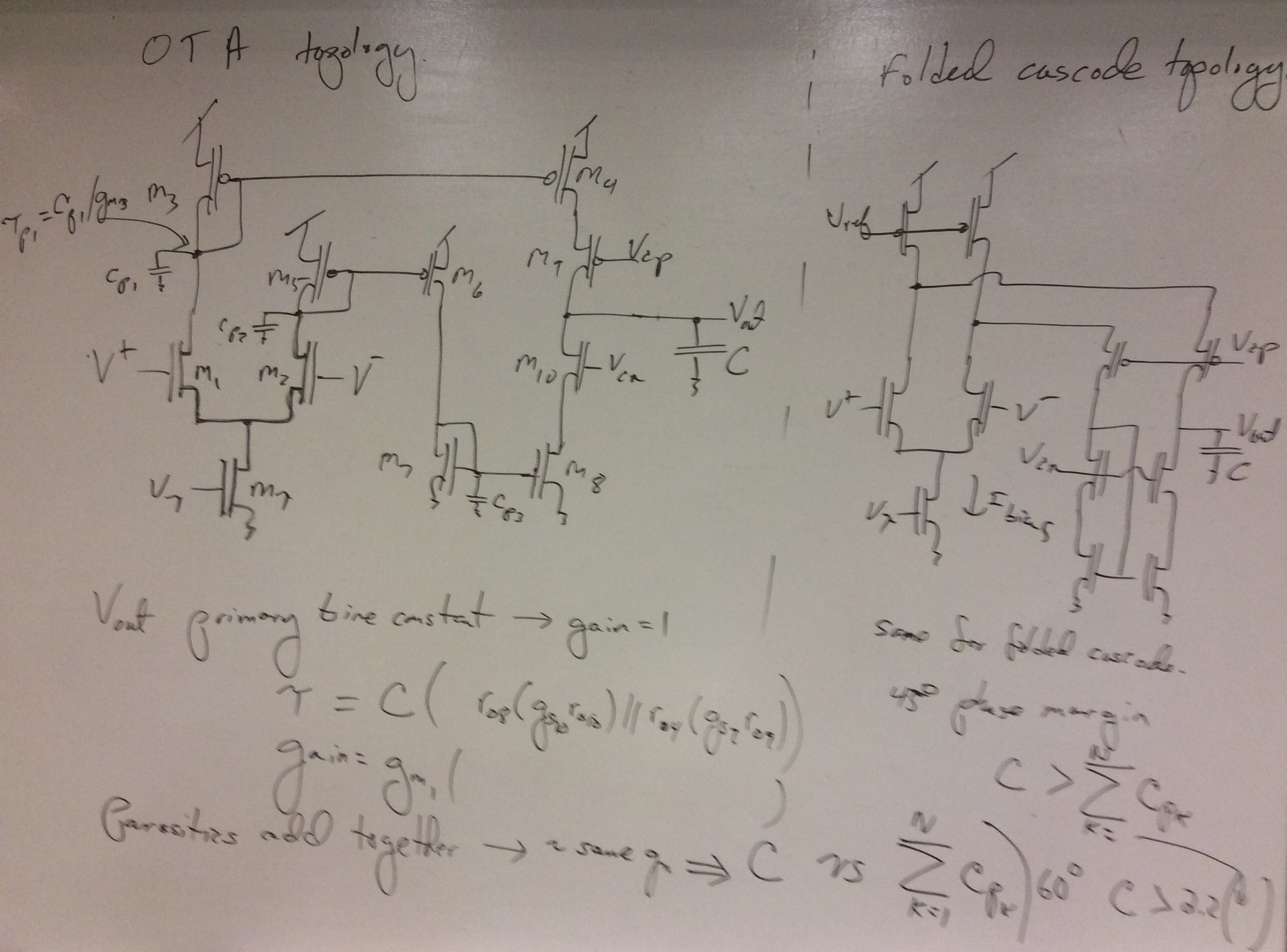
You will primarily use transistors for your circuit design. You may not use OTA devices, unless explicitly specified in the design, for the design of your amplifier. Your previous (accurate) simulation parameters are required for this project (EKV based, scilab/Xcos). You are allowed to use Floating-Gate (FG) transistor devices available in the FPAA if desired.
Capacitance Modeling can be found from the resulting routing.
Area and Power must be calculated and minimized.
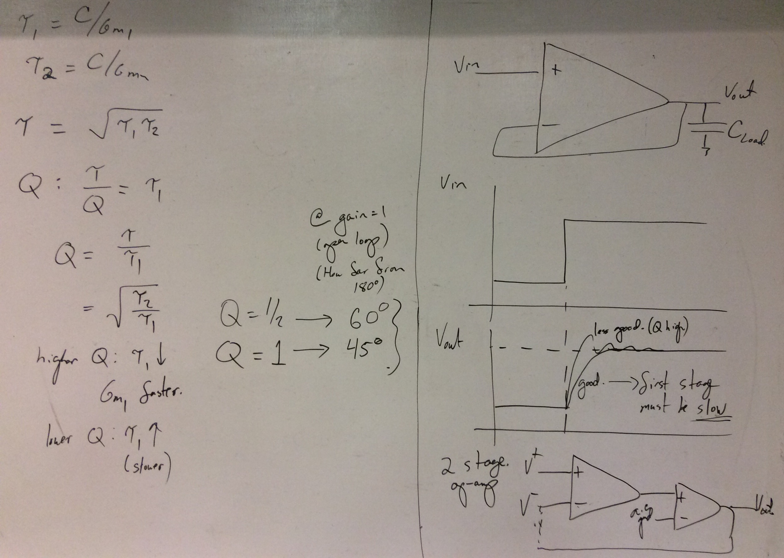
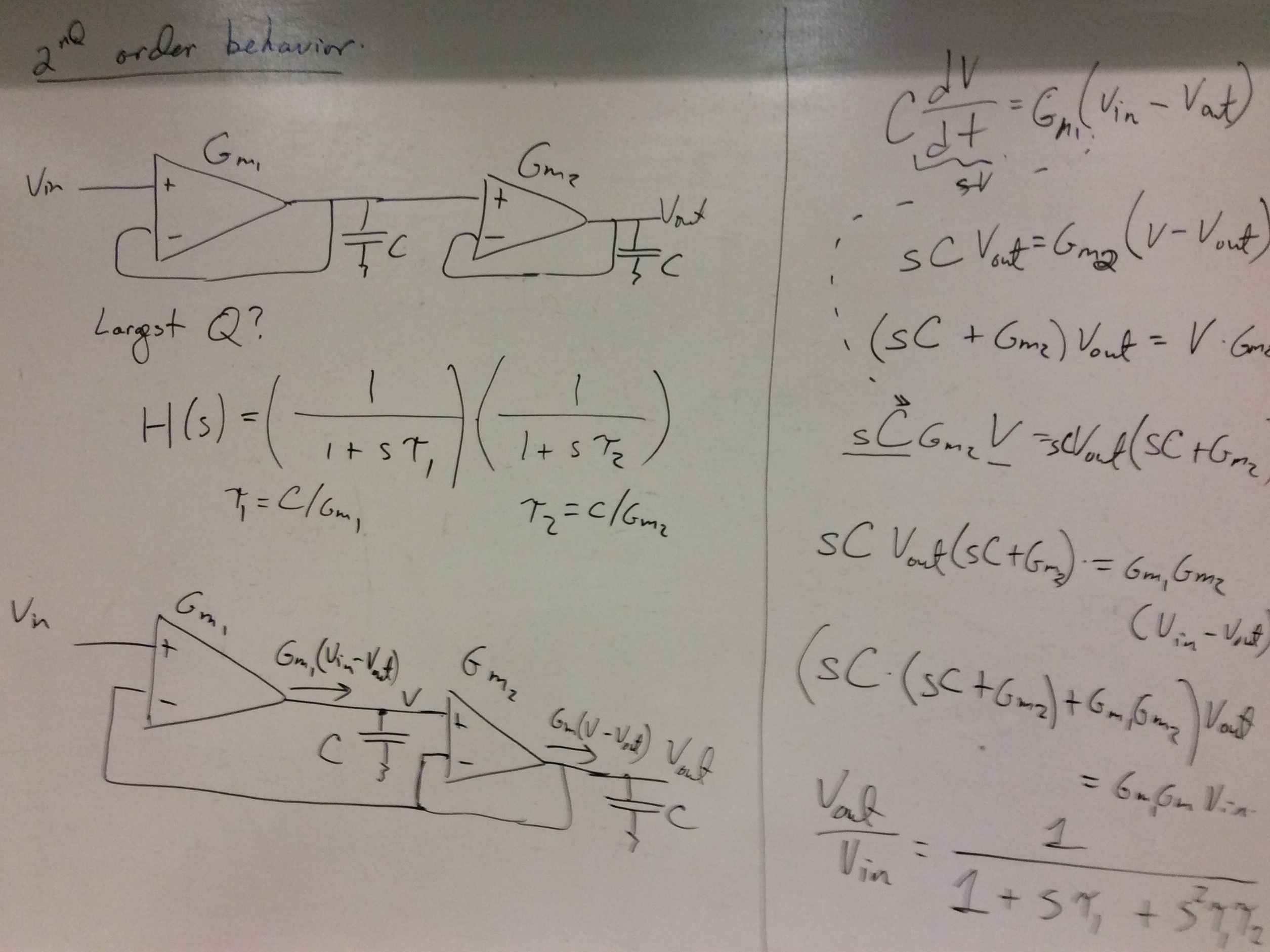
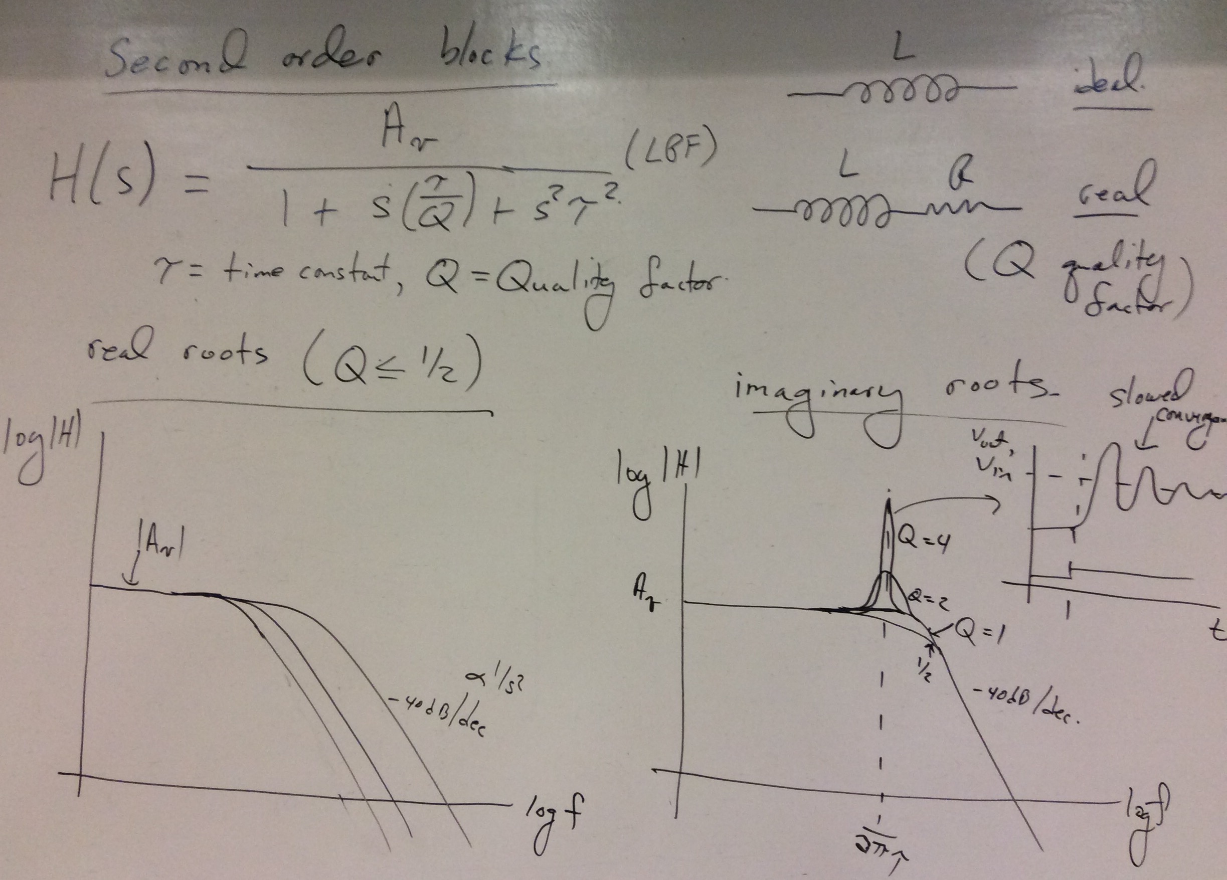
The common specifications for all designs; the design is a differential input, single-ended output amplifier. The common specifications are
In addition each group will be assigned for additional specifications; these specifications will be sent by email to the class. These specifications include
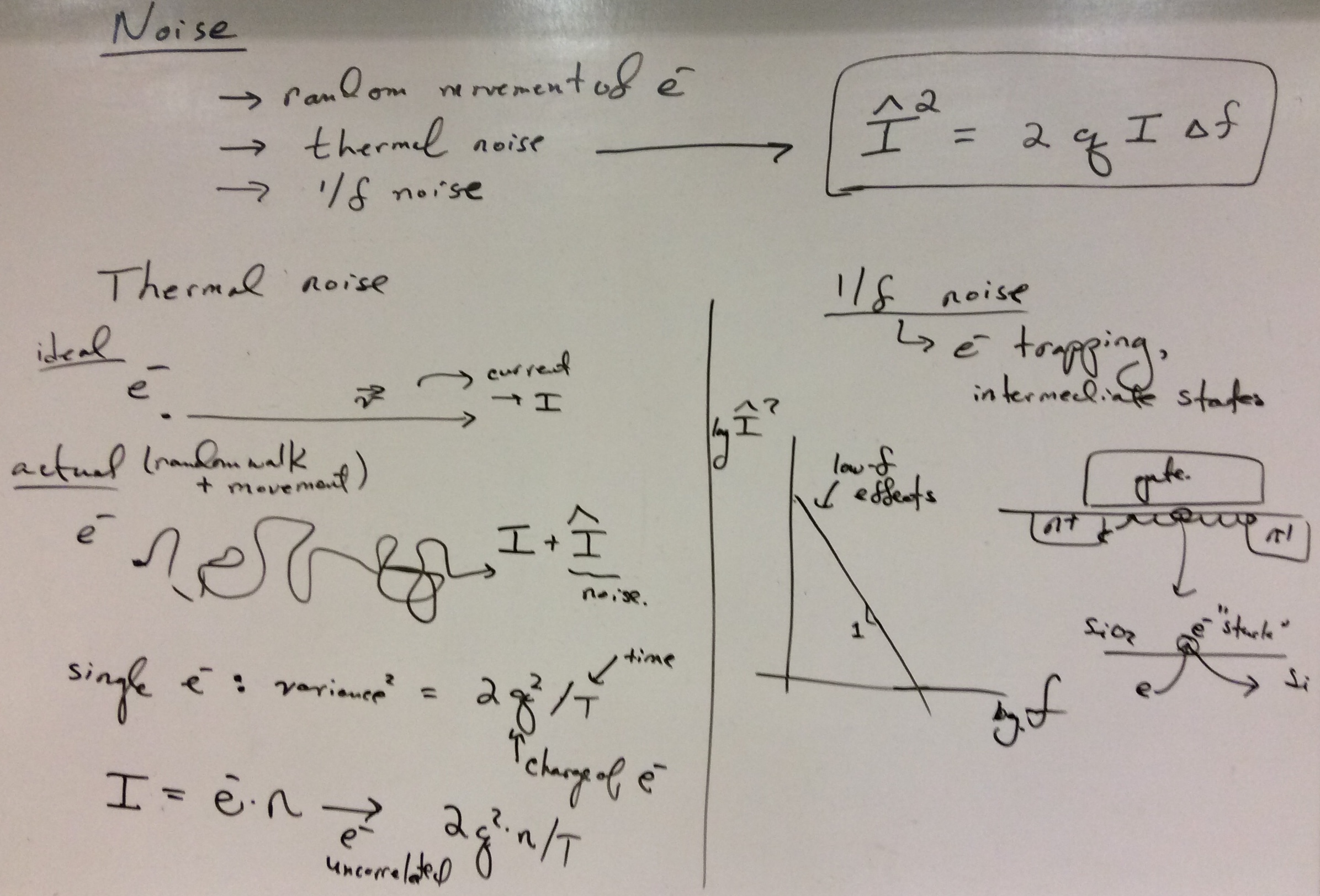
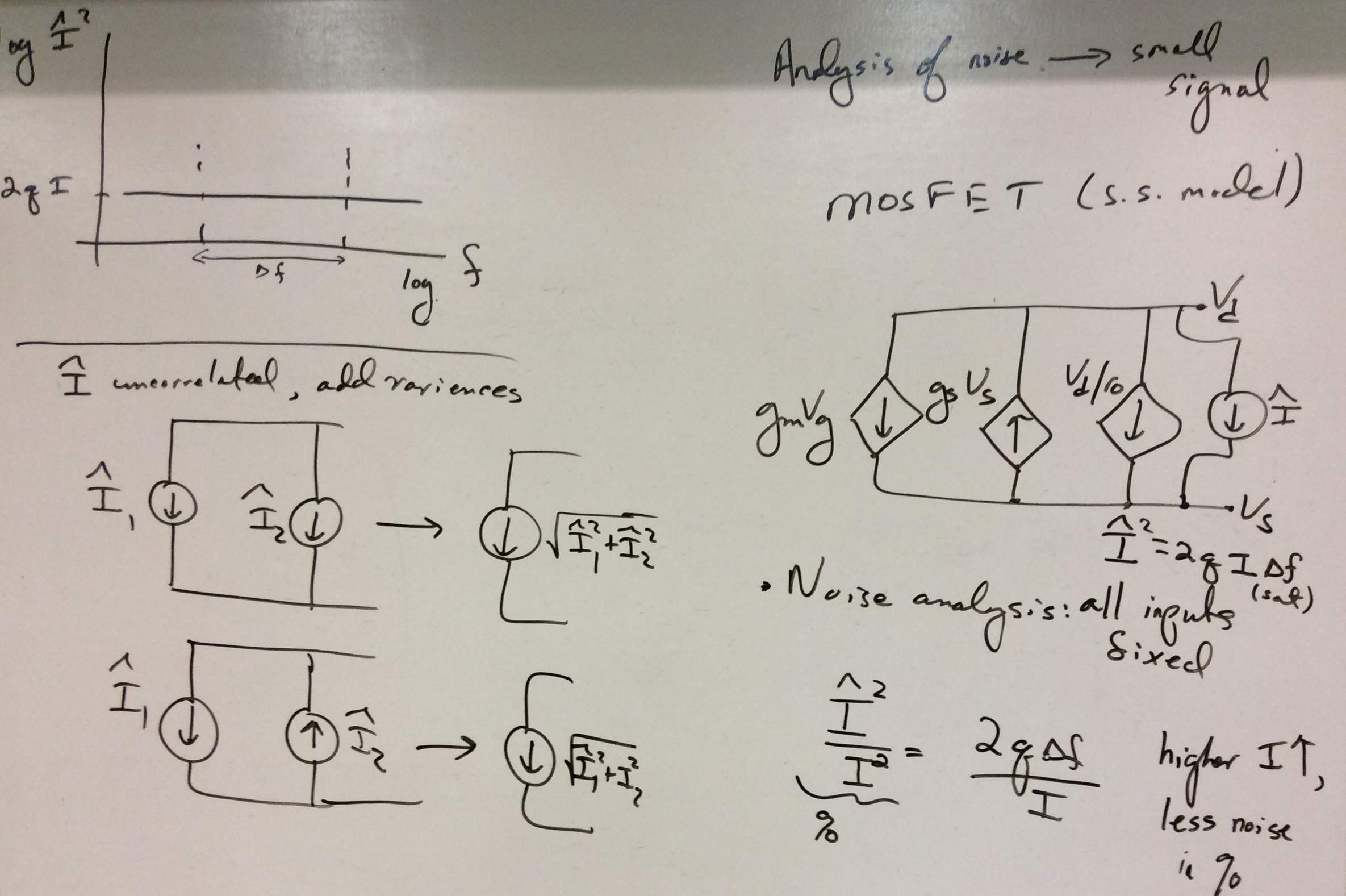
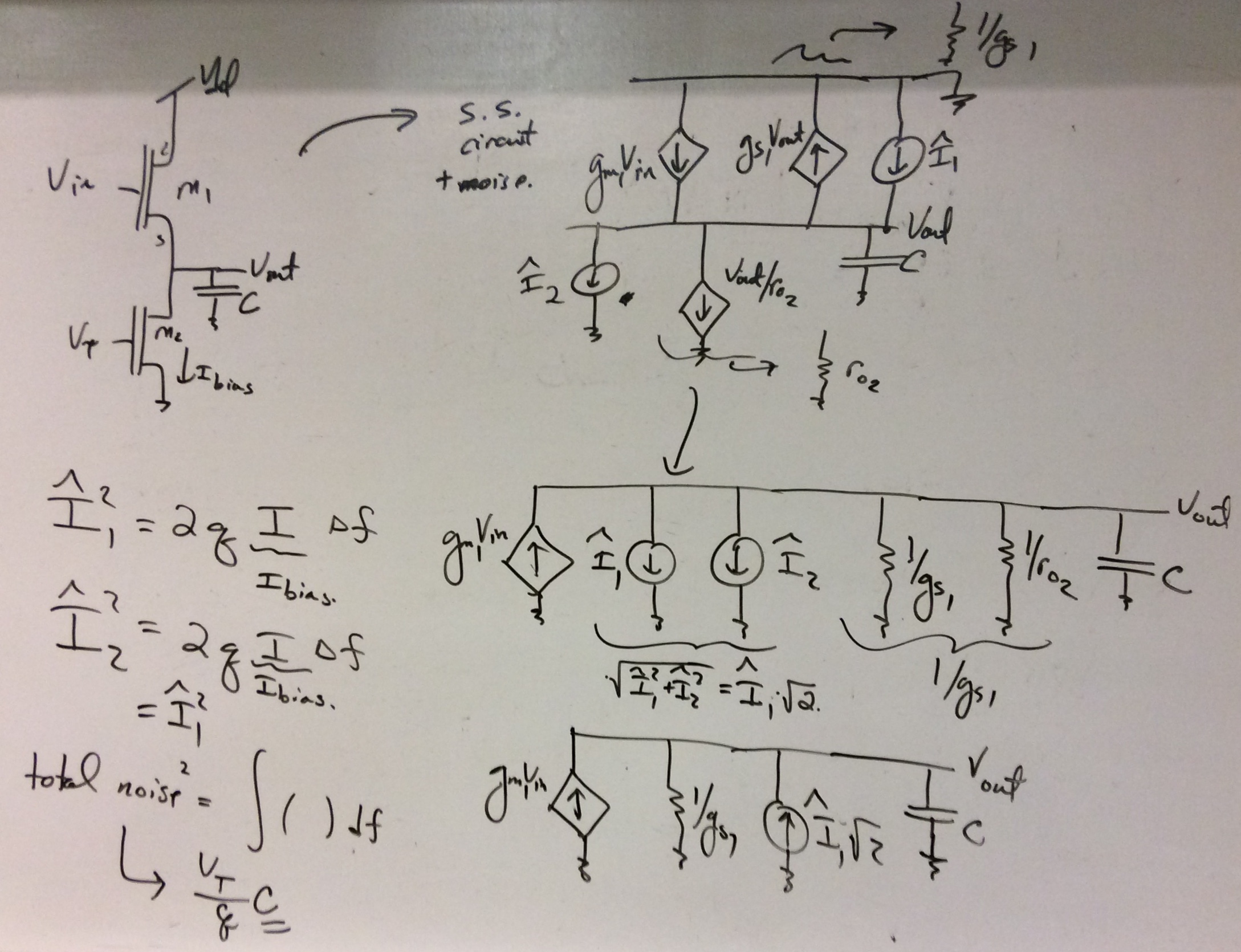
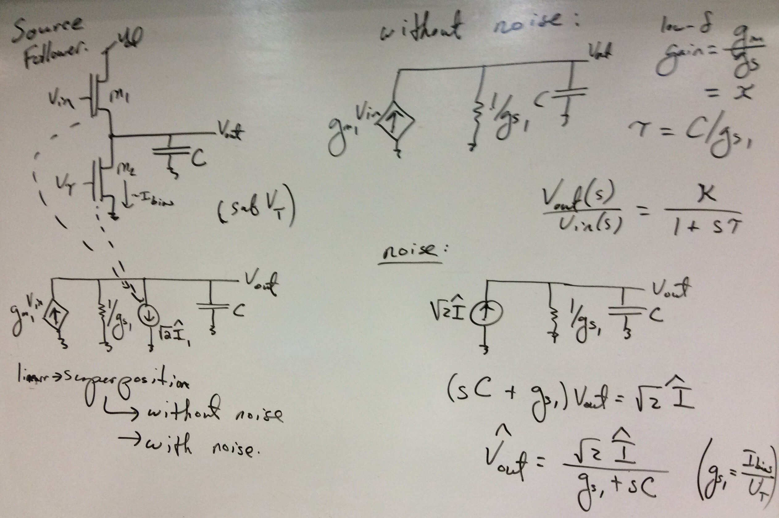
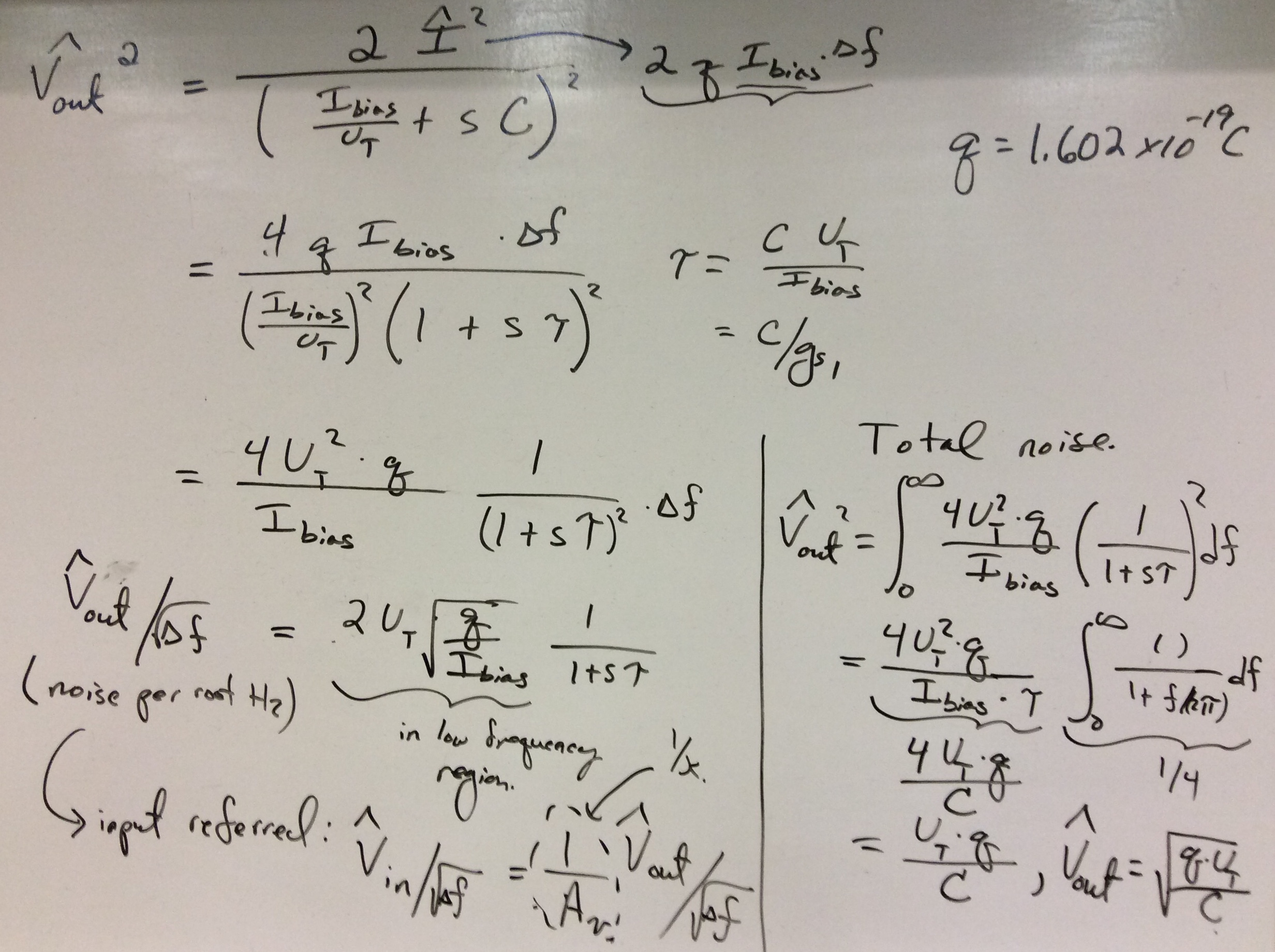
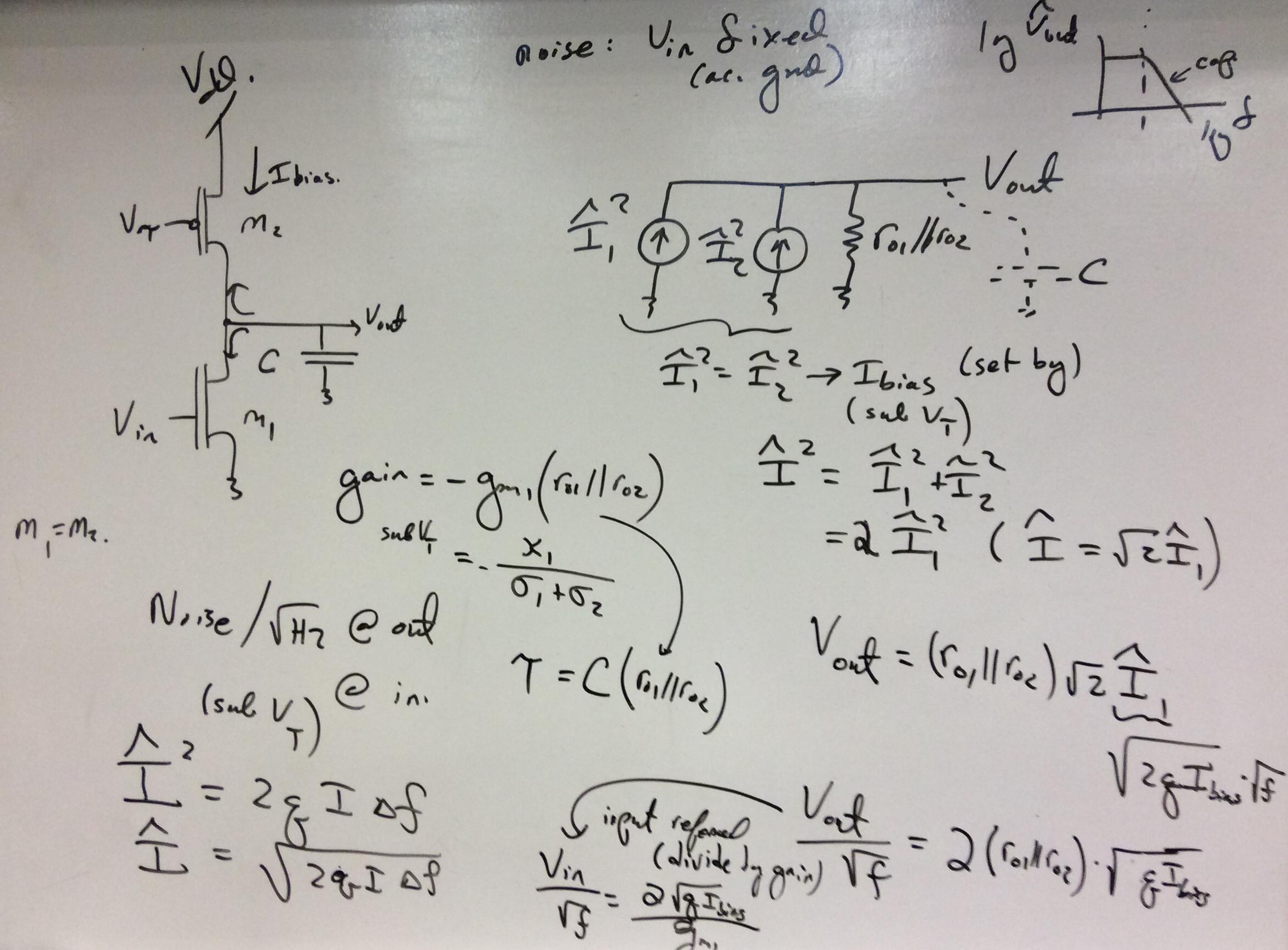
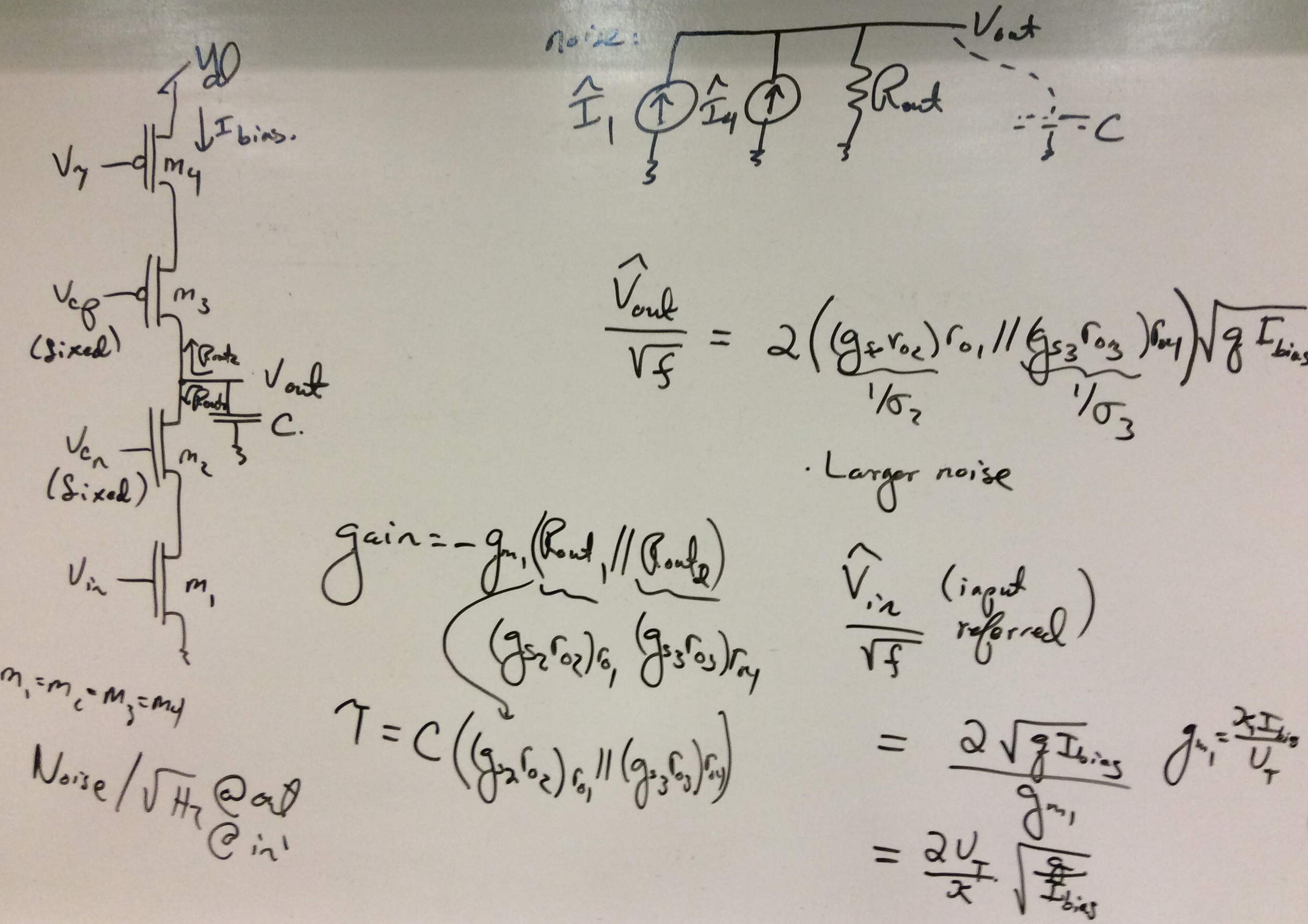
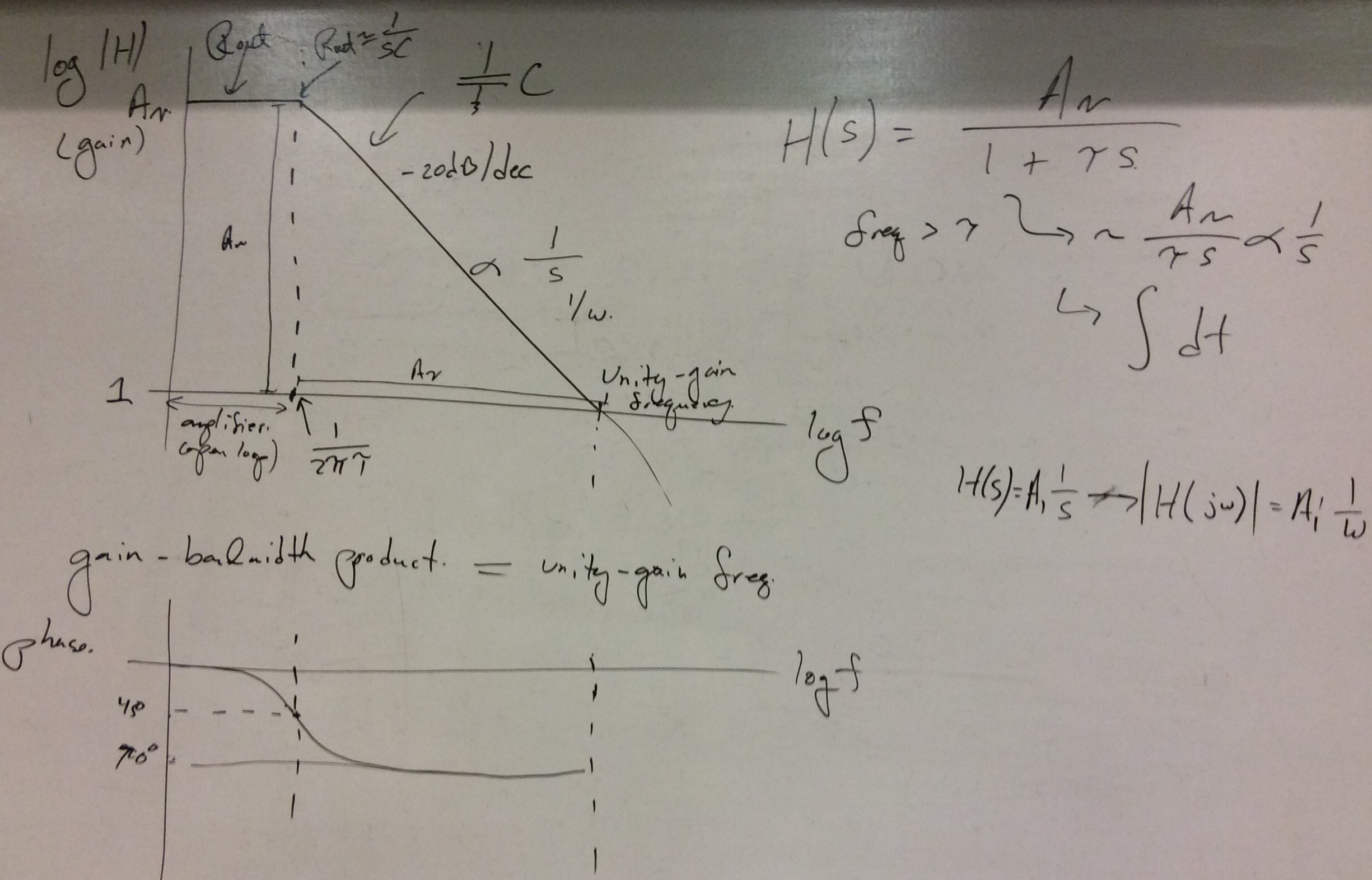
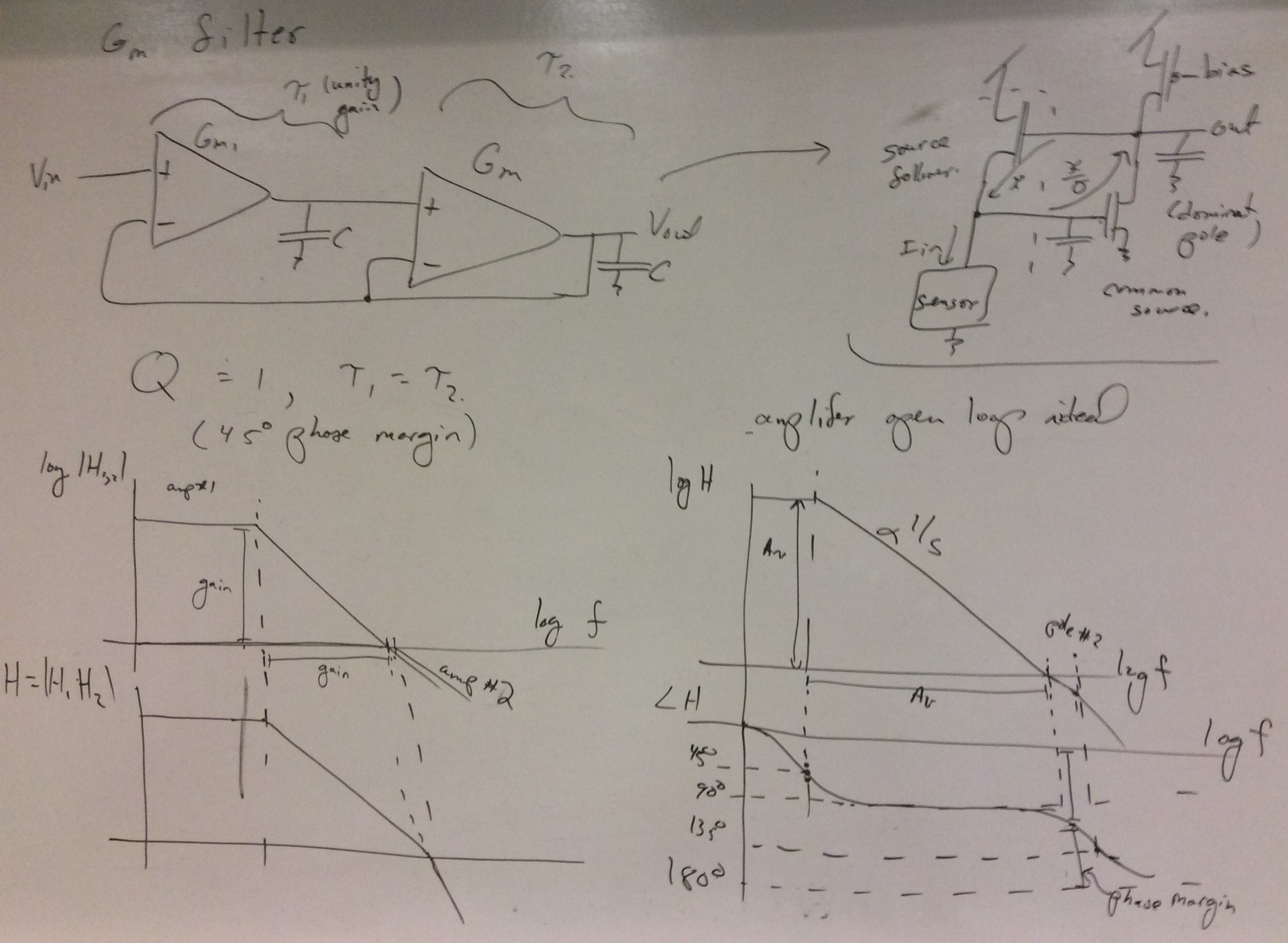
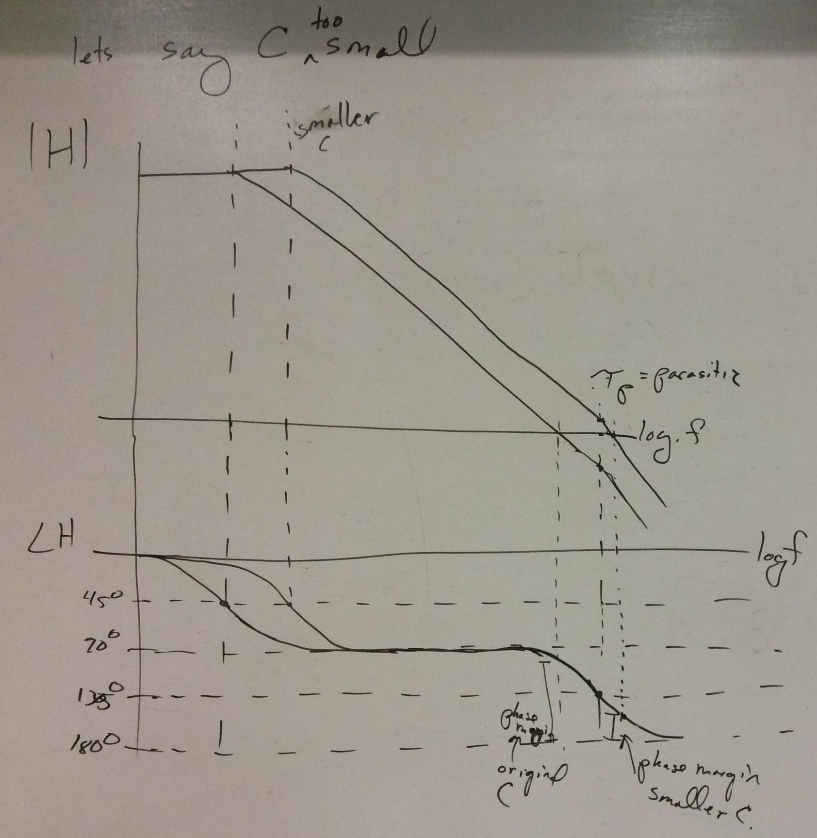
The noise measurement is input referred, that is, if one has an ideal noise voltage source, it would appear in series with either the input to the positive or negative terminal. Typically from SPICE for a noise measurement, you will get noise / rt(Hz) at the output (we are only assuming thermal noise for this project), so an approximate measurement is to divide by the lowest in-band gain (you have a given -3dB frequency, so take the lowest gain in that region) to get your input referred noise / rt(Hz).
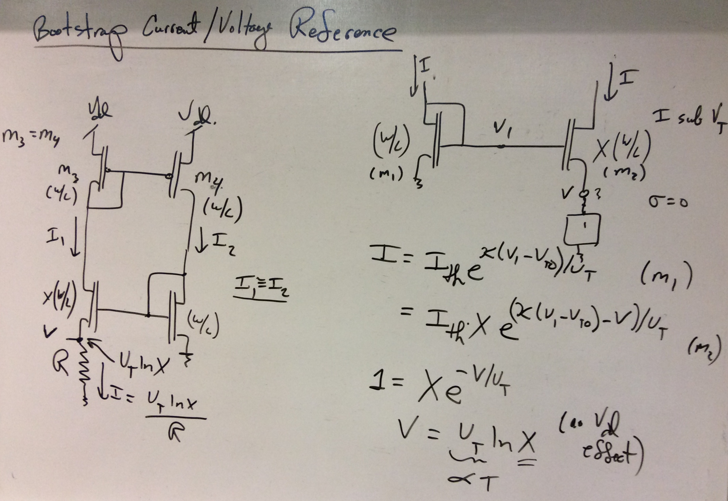
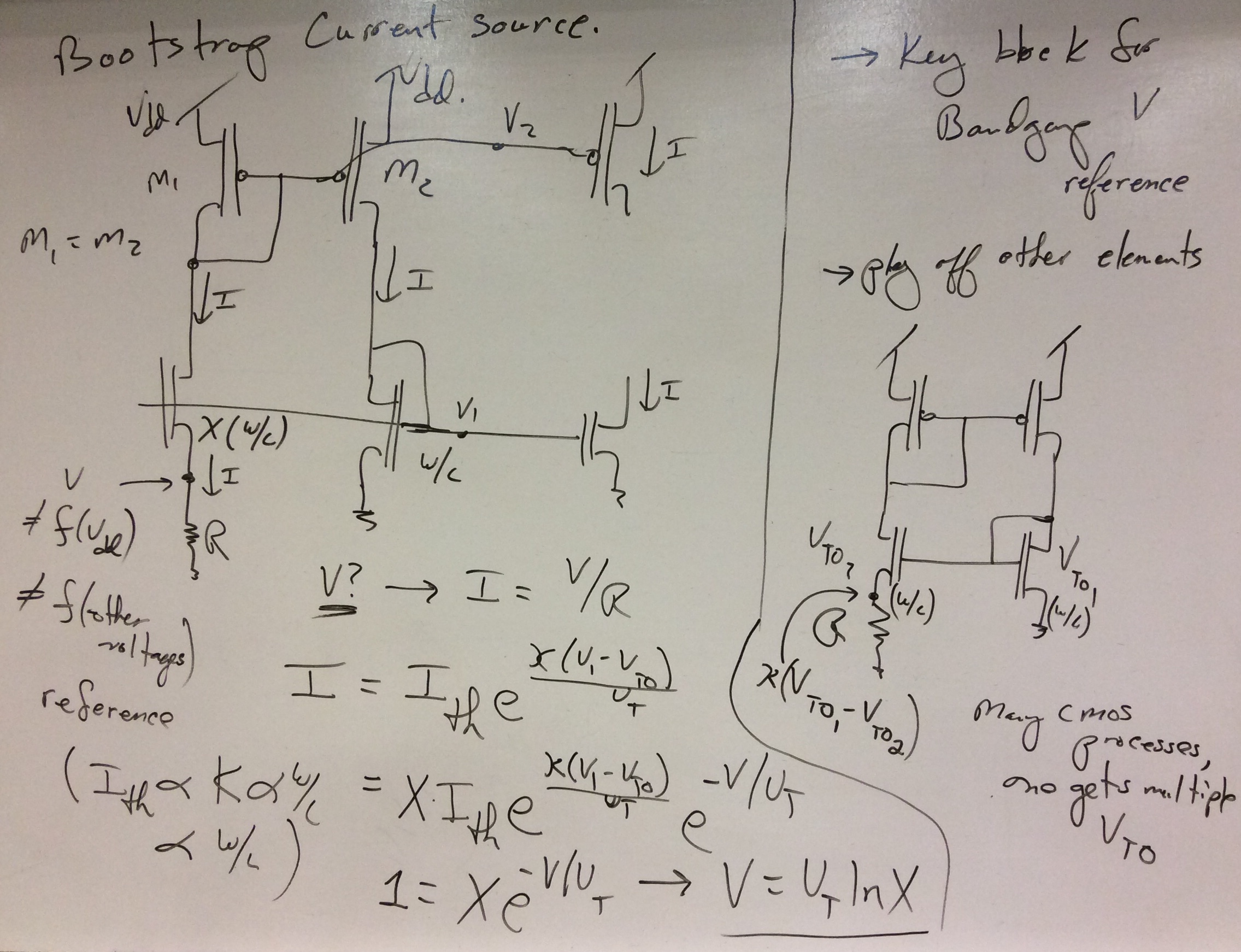
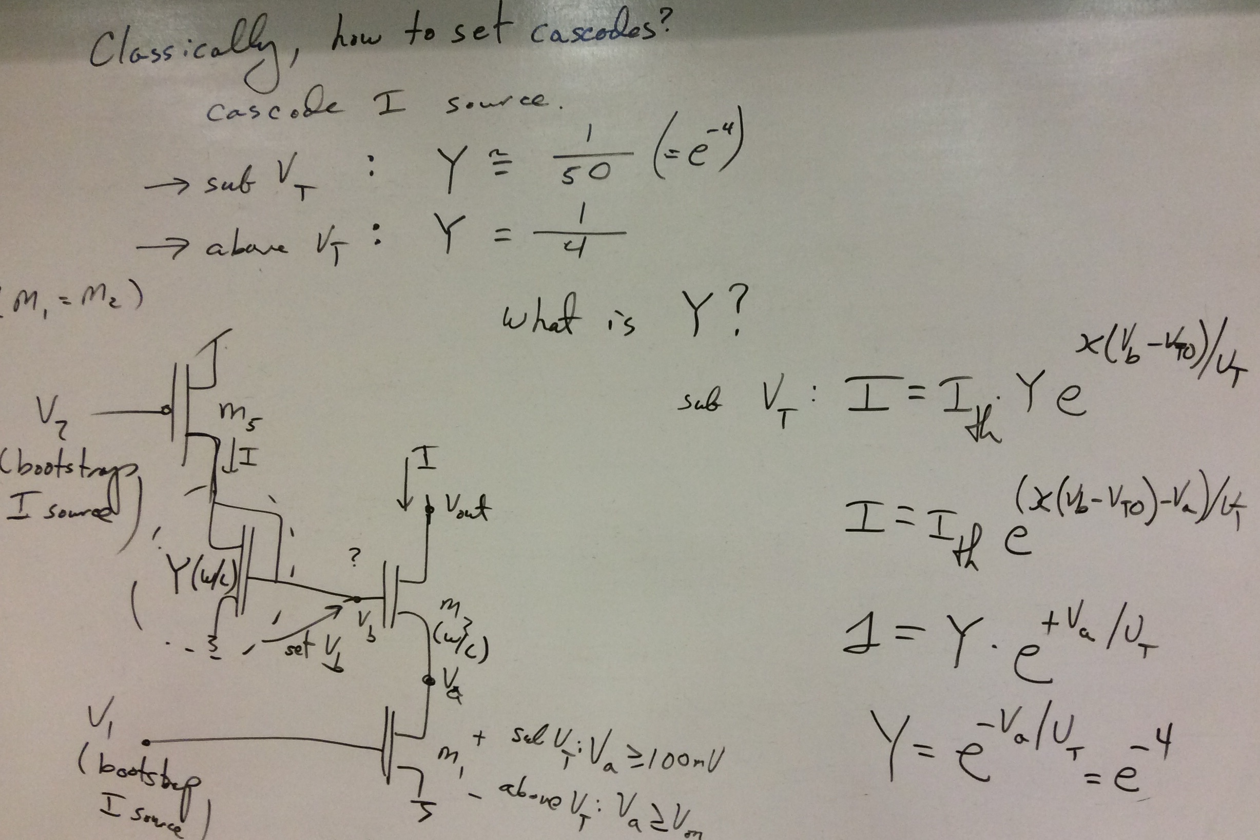
Remember that you will need to provide all biases on chip. Yes, the device has multiple DACs, but I would not advise using them for your design (can use them for setting the inputs for testing your design) both in terms of area, power, and temperature effect issues. You will need to bias the components in your design, and you are allowed to choose one resistor (as desired for your biasing) for the design. One strong suggestion would be to use a bootstrap current source generator, and use this circuit to bias any cascode elements, if desired.
Your presentation will include the table of all specifications and what specifications you achieved with the resulting data. You need to insert your target numbers for your unique specifications (4 of them; I will check that they are correct). Of course, you need to have supporting evidence for your specifications.
In your presentation materials, you need to include: