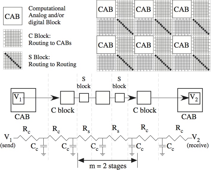
The figure below shows the basic Manhattan based routing structure used for our SoC FPAA device. The routing fabric in this architecture is both useful for computation as well as switching, particularly for local CAB / CLB routing as well as in the "C" block routing.

The SoC FPAA enables programming experiments that characterize the fundamental properties of the configurable fabric by experimental measurements on the configurable routing fabric. The figure below illustrates compiling (and measuring) two circuits to characterize precisely the behavior of these circuits, including load capacitance of the fabric itself. This FPAA structure facilitates the direct characterization of the resulting capacitance. One can directly predict delays along each of these lines. Every experiment uses the same voltage biasing, fixing the capacitance of p-n junction devices throughout this experiment. The resulting measurements give a measurement of the resulting routing capacitance, as well as enables, through the routing fabric, a range of tunable capacitor blocks. Precise measurement of routing capacitances enables tuning, through programming switches, for precise capacitances where needed for matching. Matching of capacitances and programmability of current sources by FG techniques dramatically reduces the effect of mismatch in small cell sizes.

The minimum capacitance for routing through a single "S" block would be routing through a local line (160fF) , plus a "C" block line (160fF), plus an "S" block line (40fF), plus a "C" block line (160fF), and then another local line (160fF). This value would be 680fF (roughly 700fF would make sense). This would be the minimum capacitance for setting up the routing.