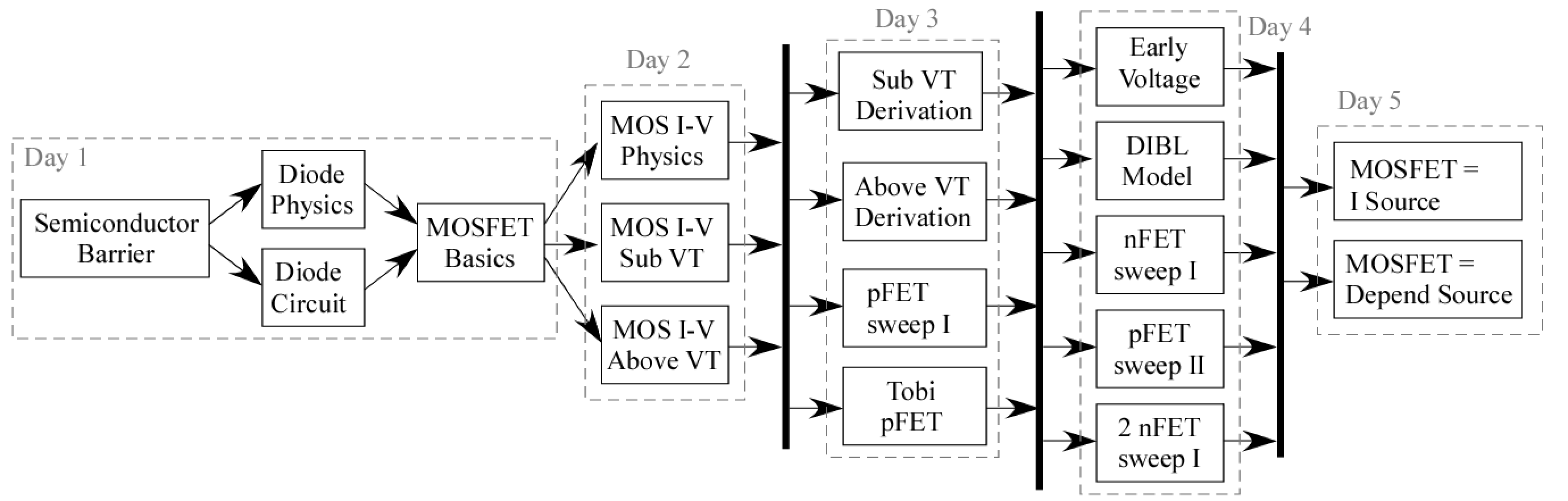
| Date | Class Topic | On-Line Lectures | Reading Material | White Boards |
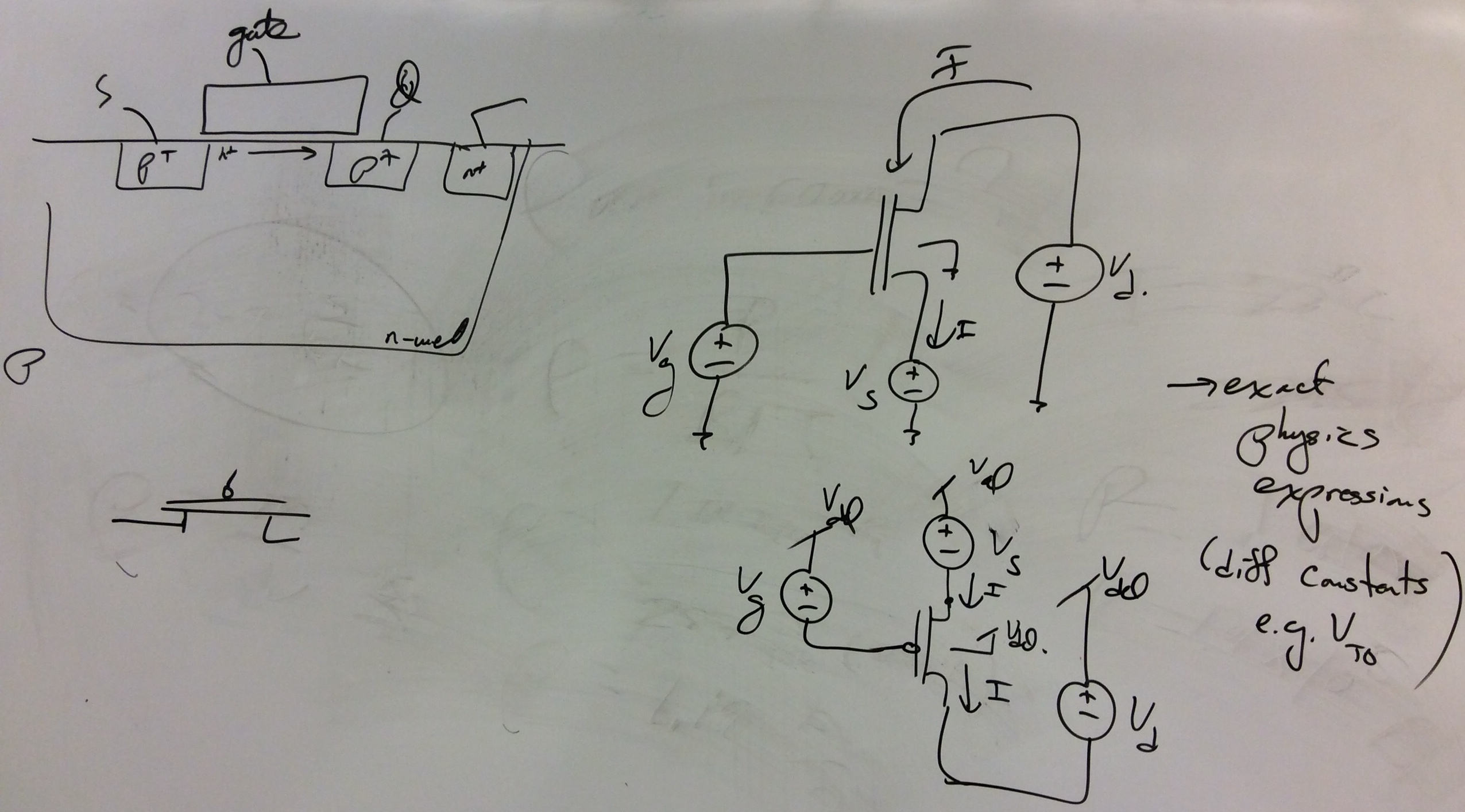
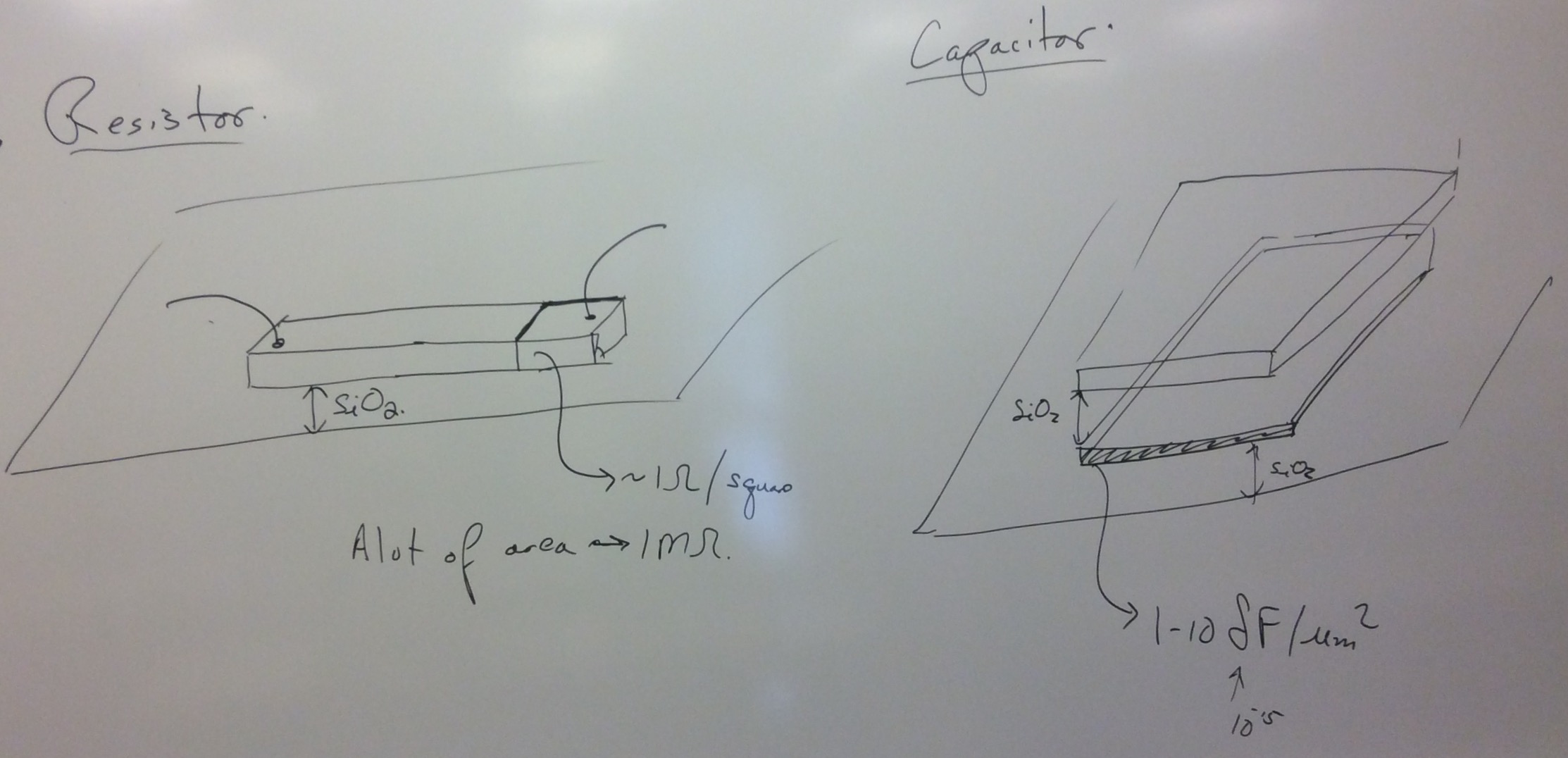
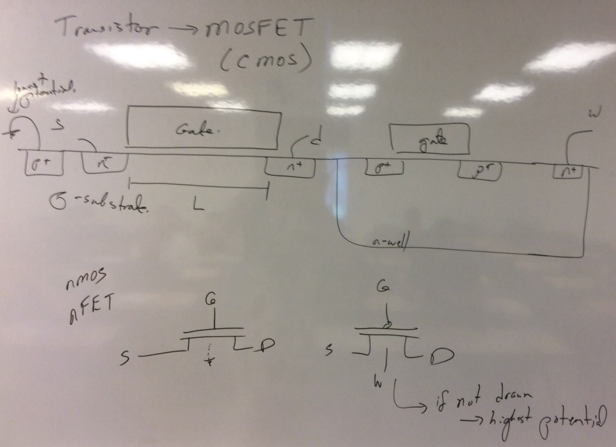
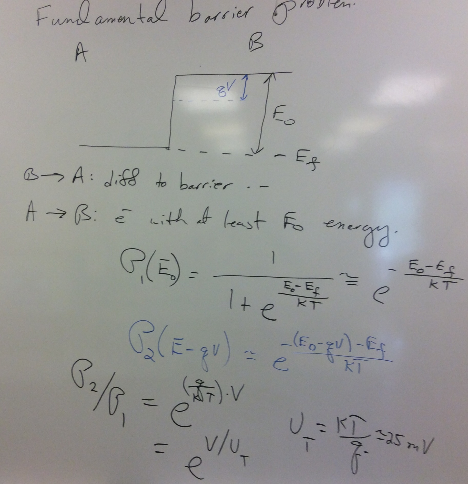
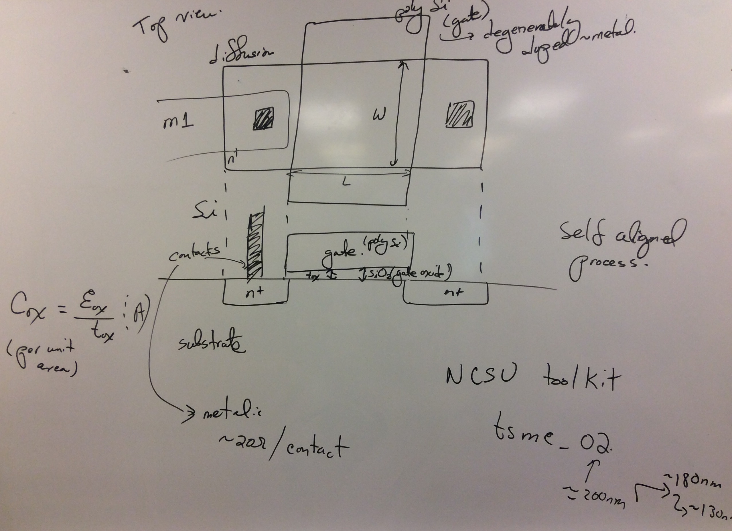
| Aug 25 | Transistor Intro |
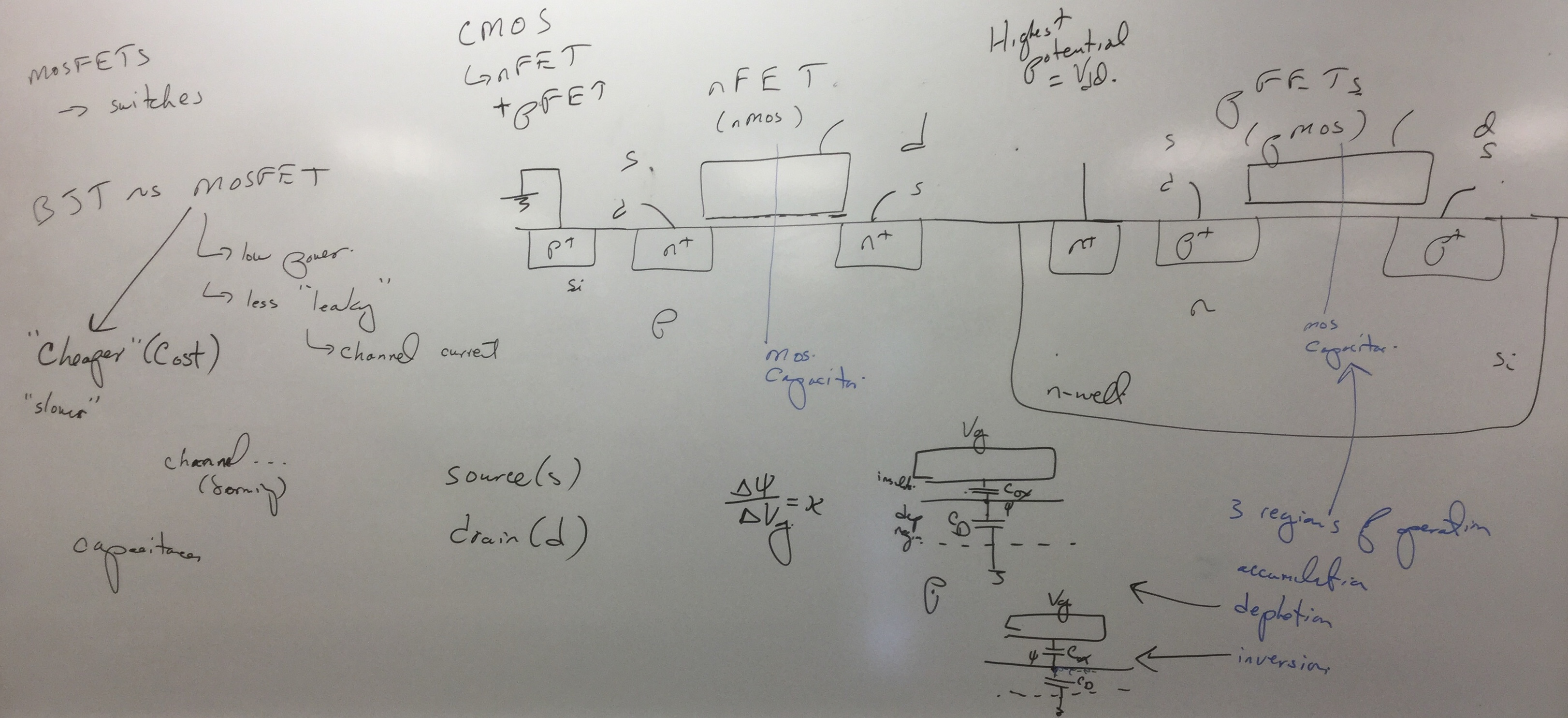
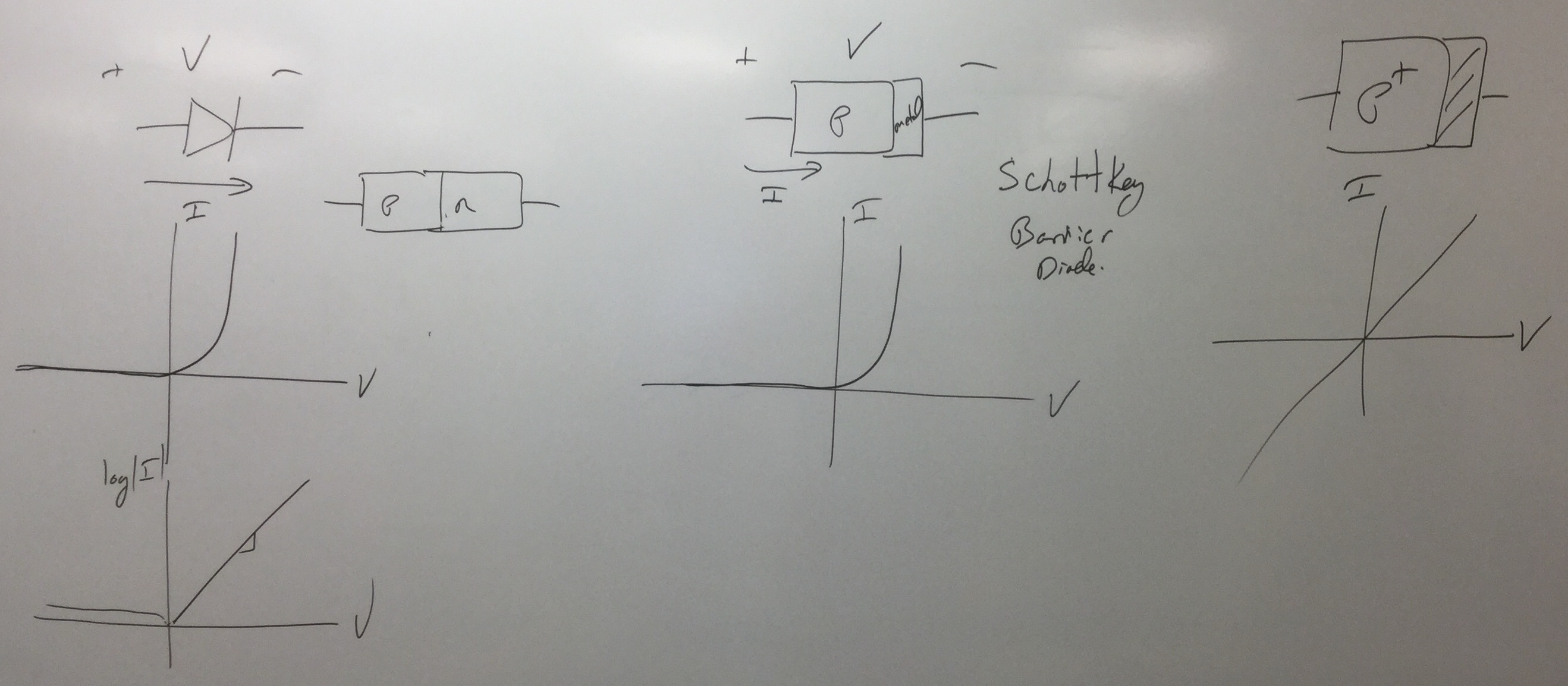
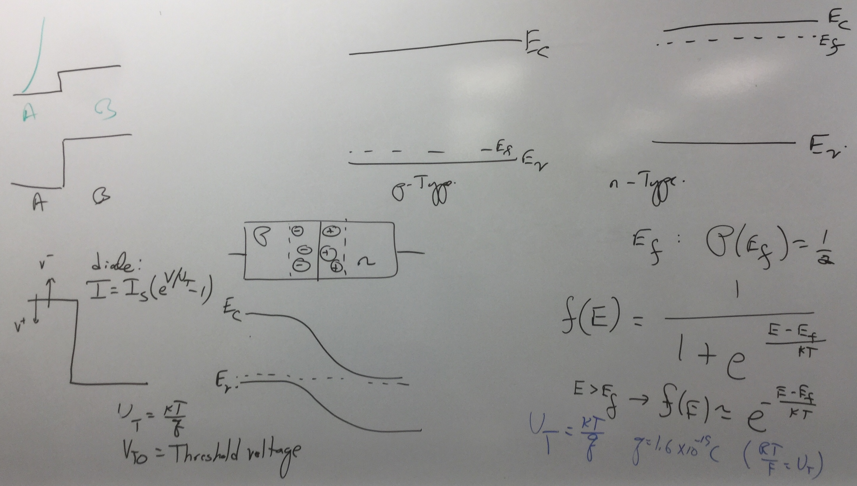
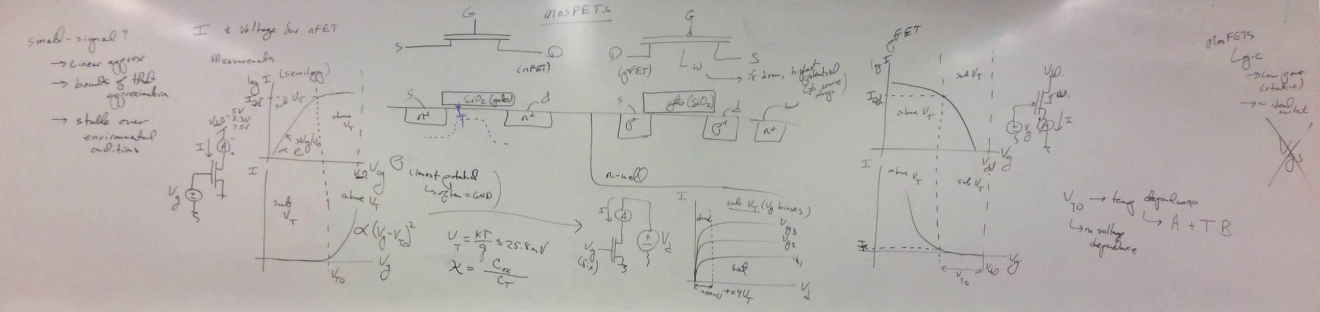
Semiconductor Barrier Diode Physics, Diode Circuit, MOSFET basics, | Device Physics Basics | 1 2 3 |
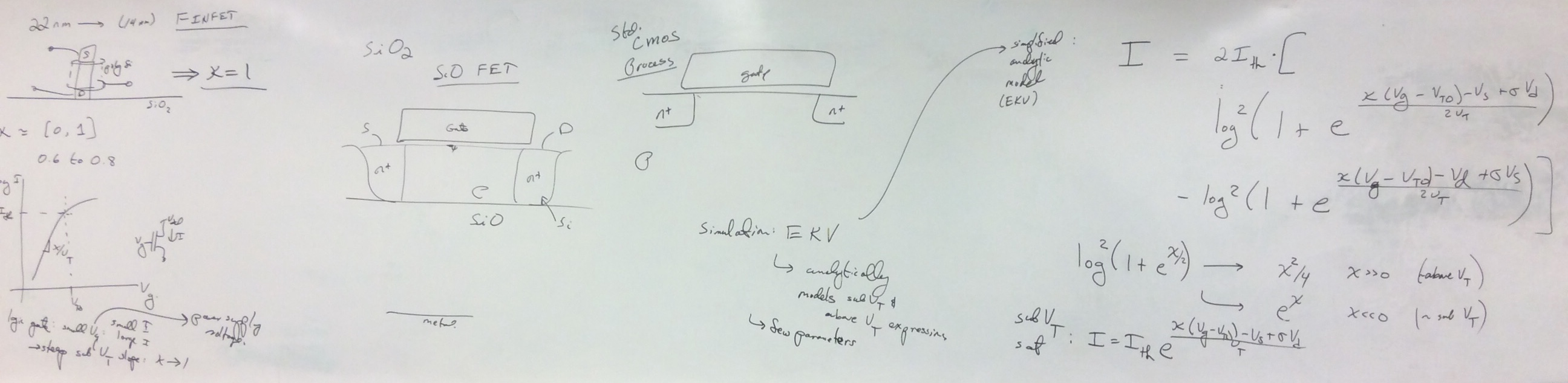
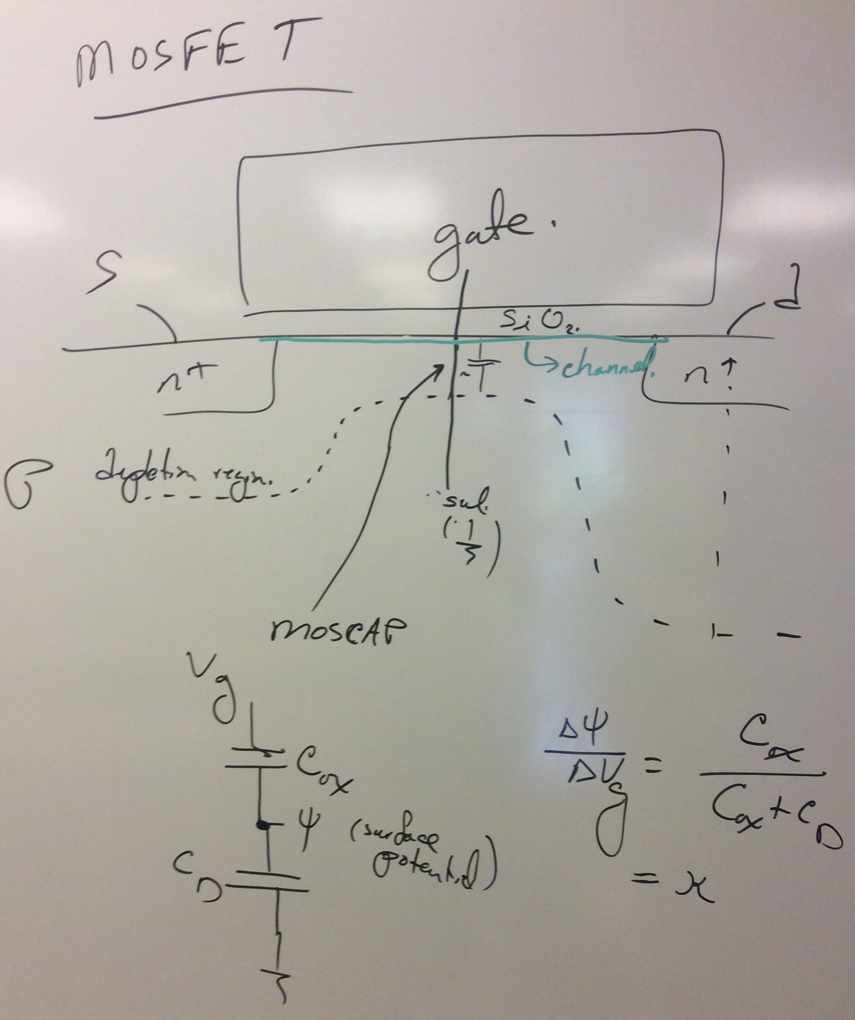
| Aug 27 | MOSFET I |
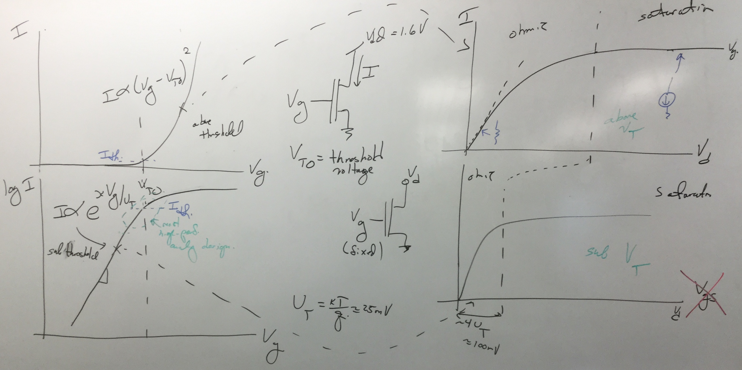
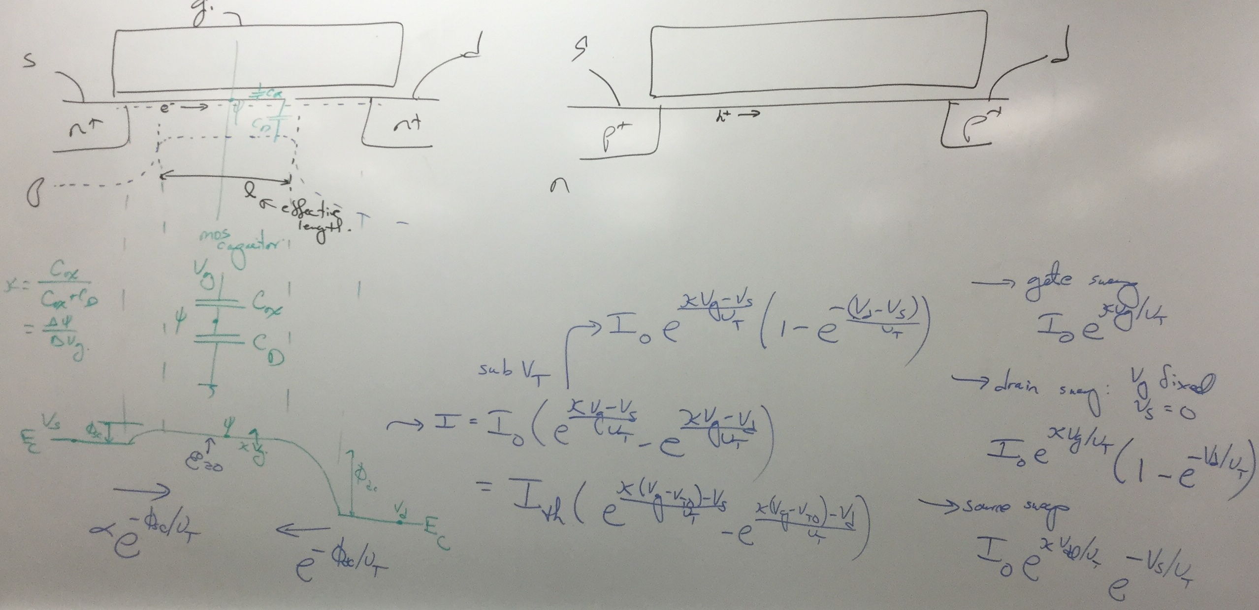
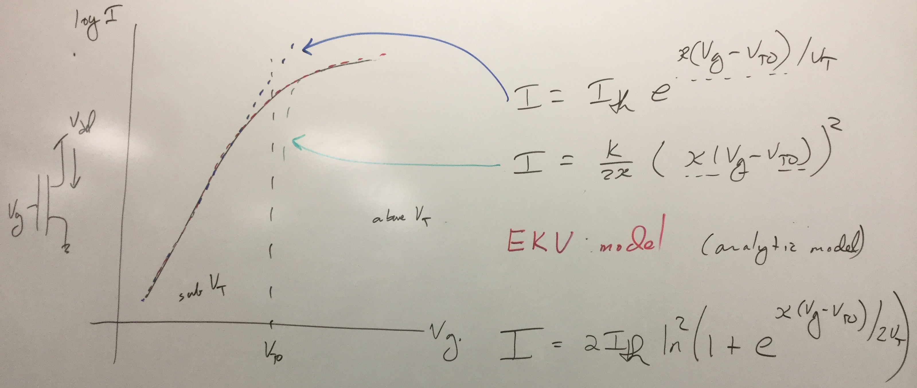
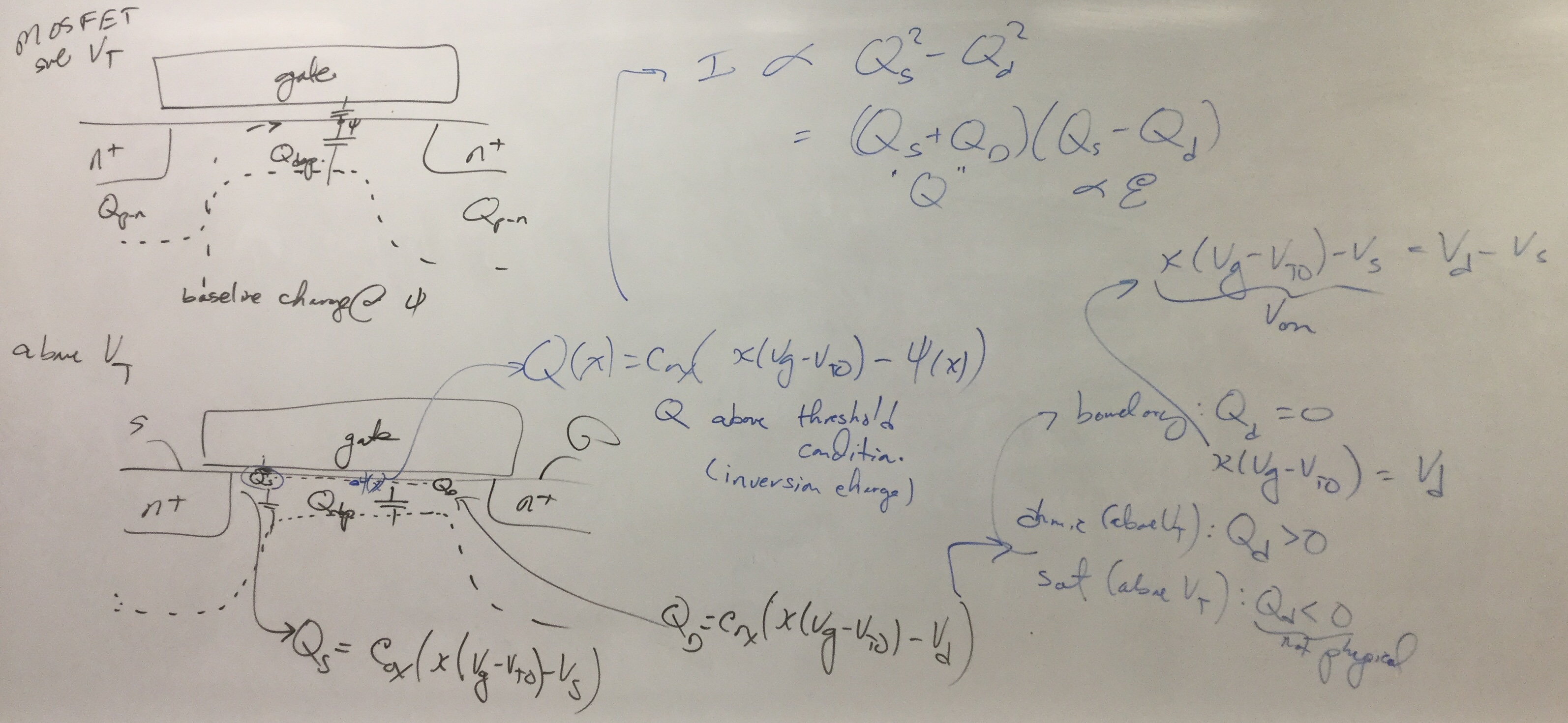
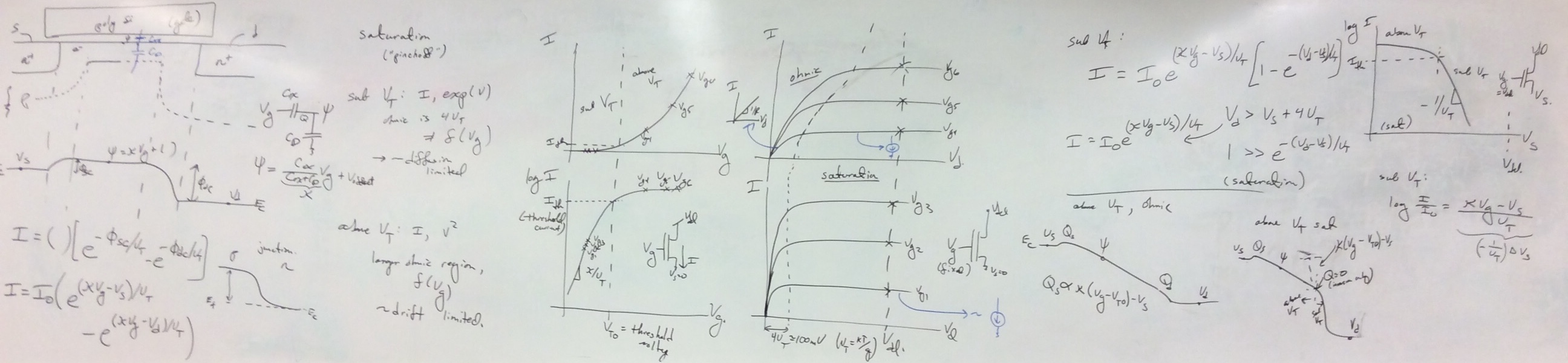
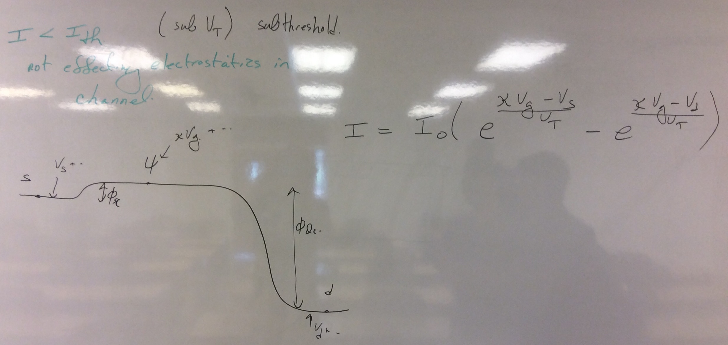
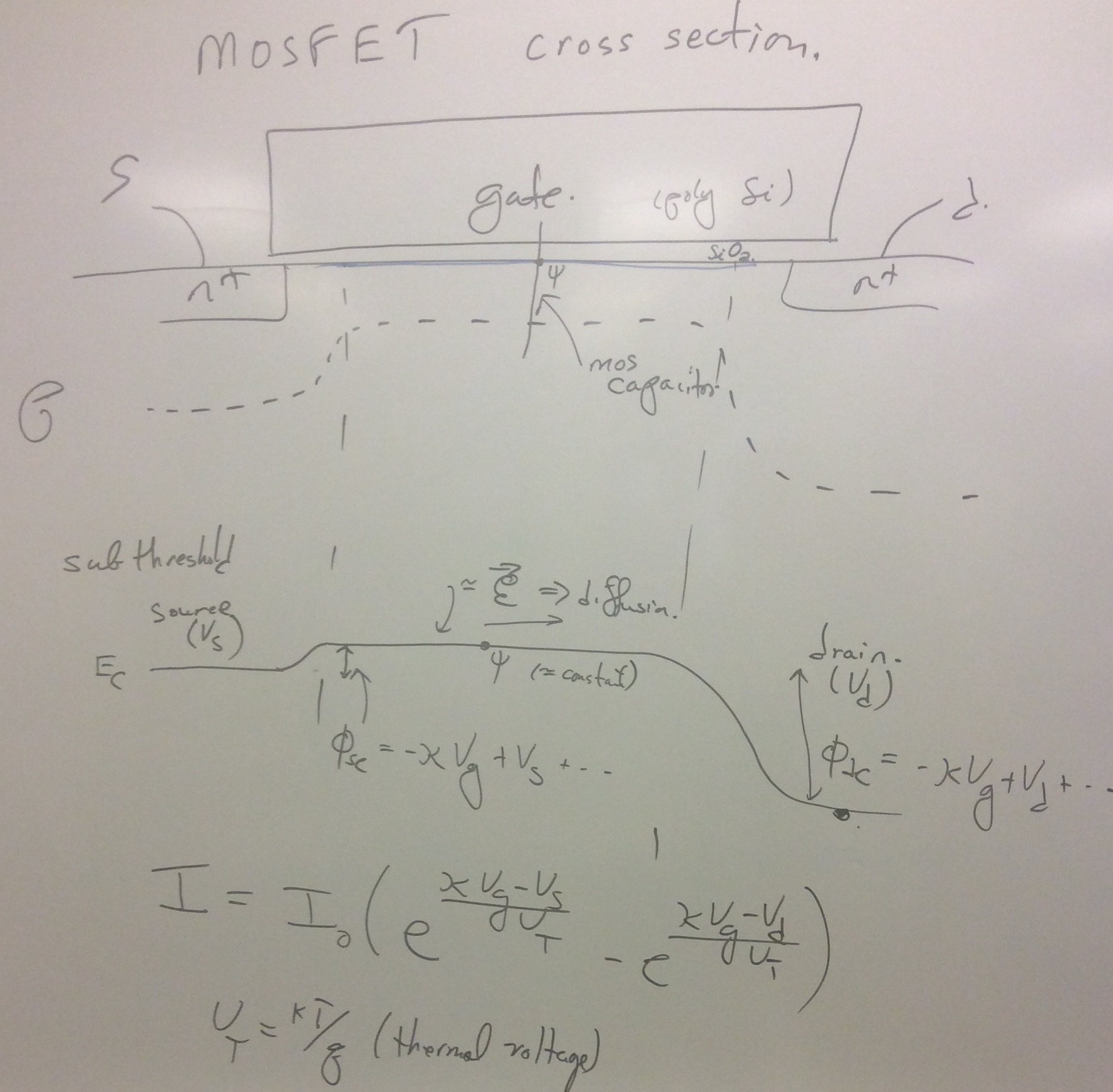
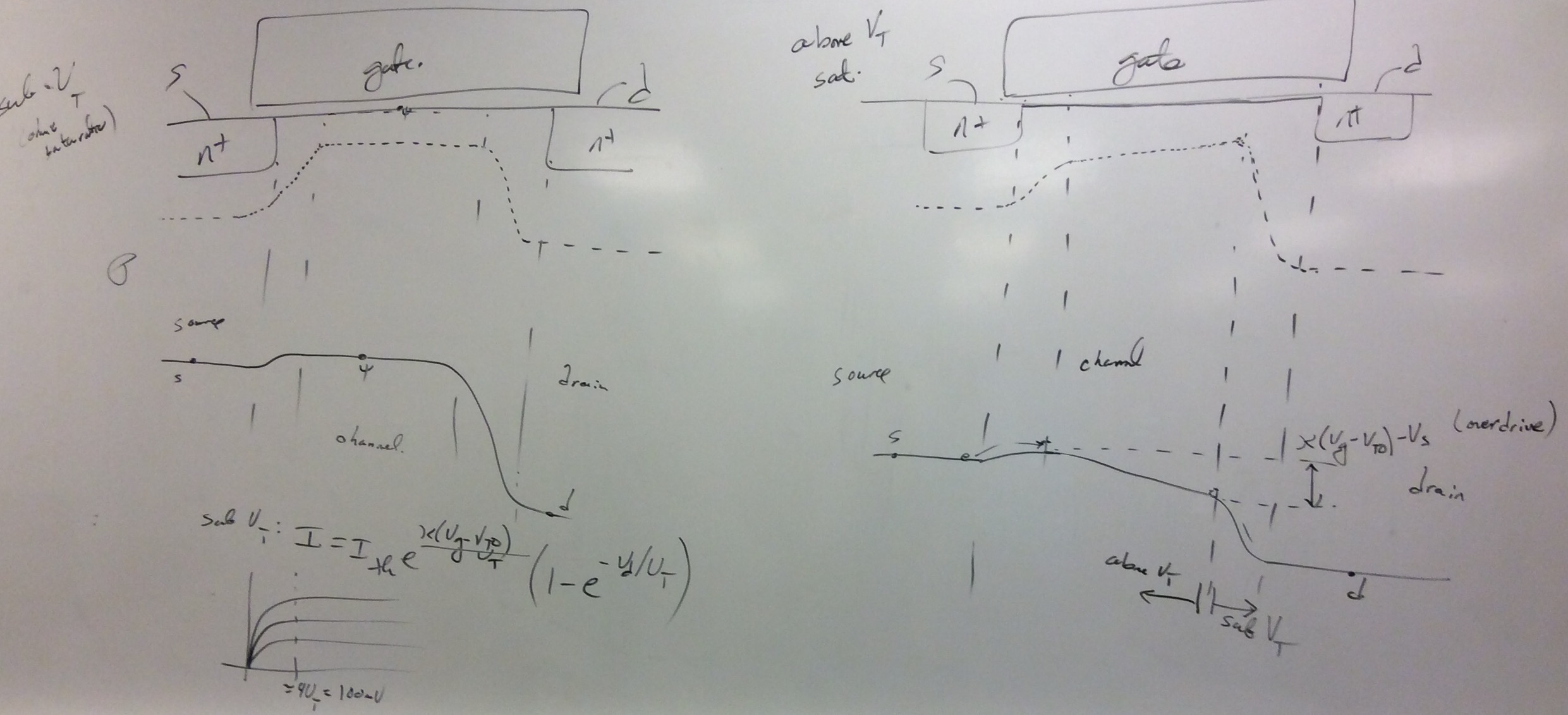
MOSFET Sub VT Equations,
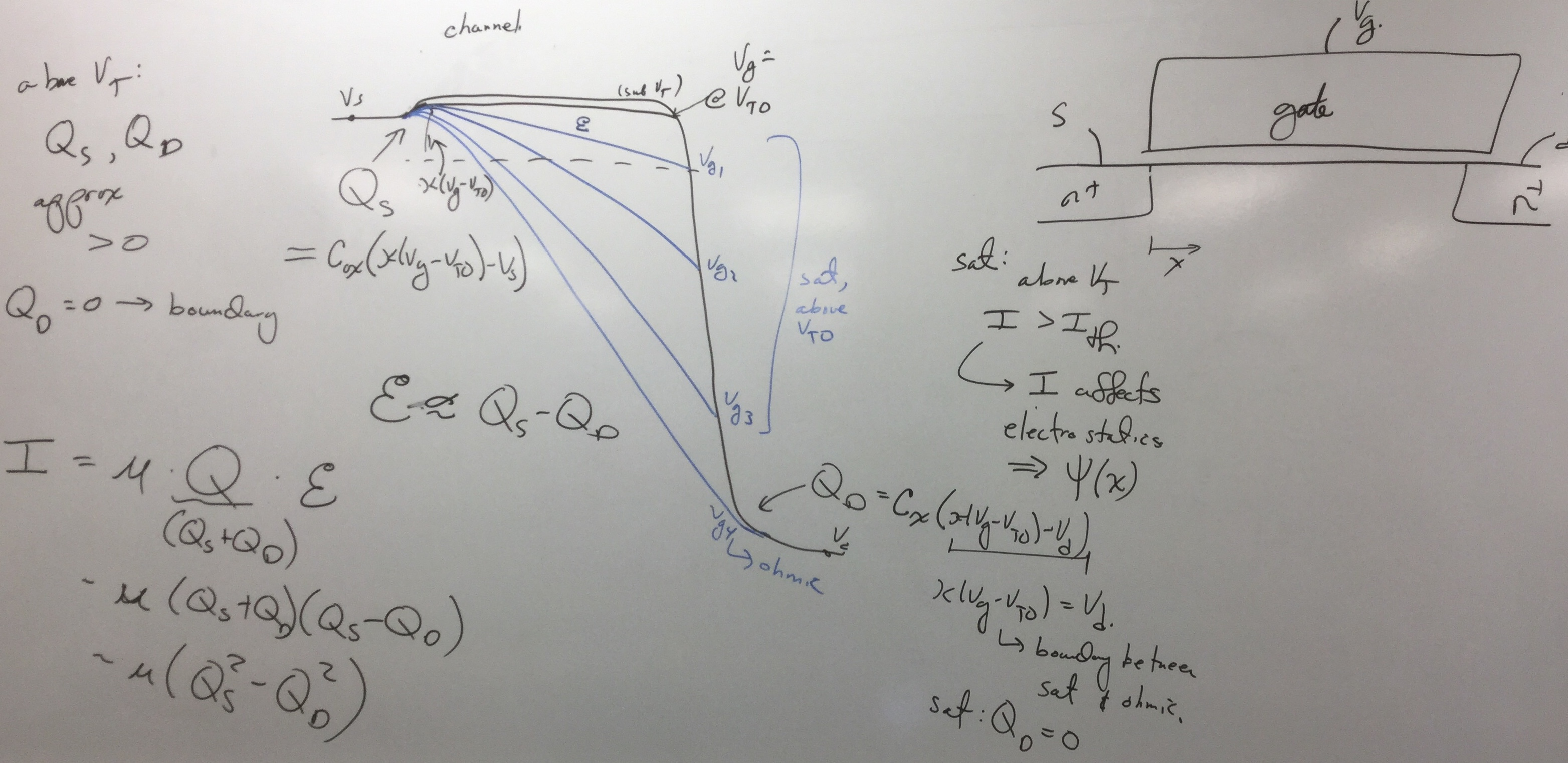
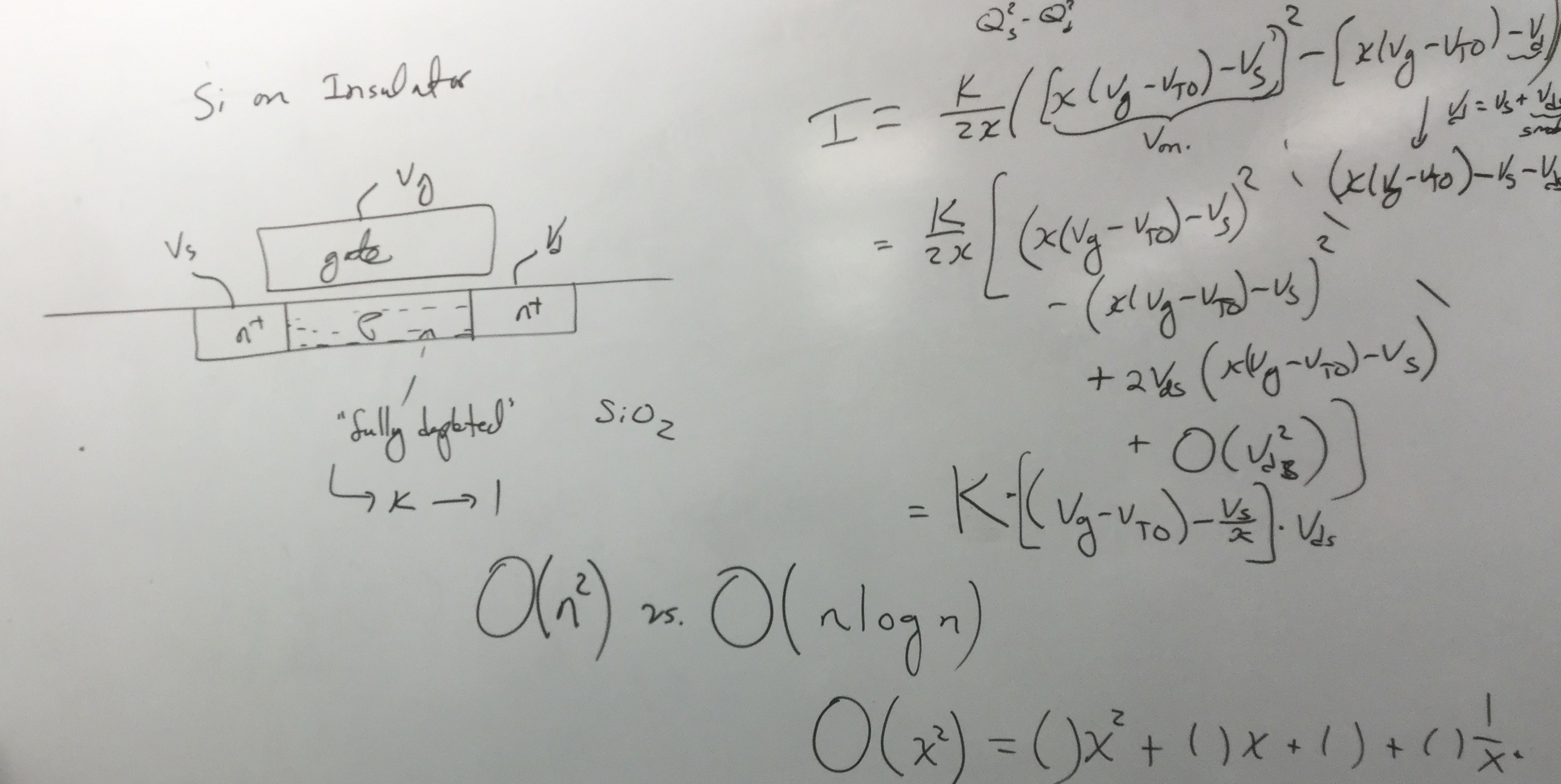
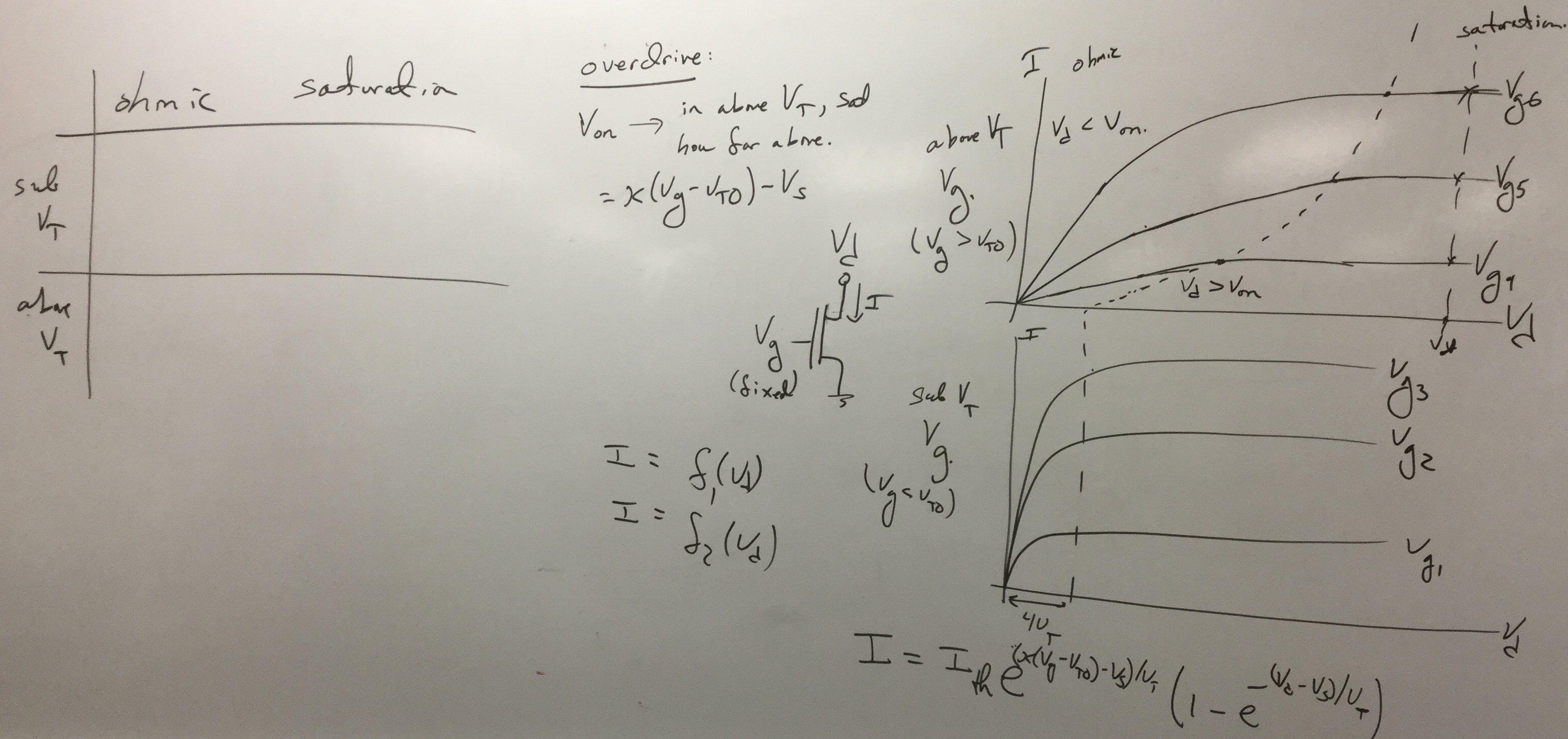
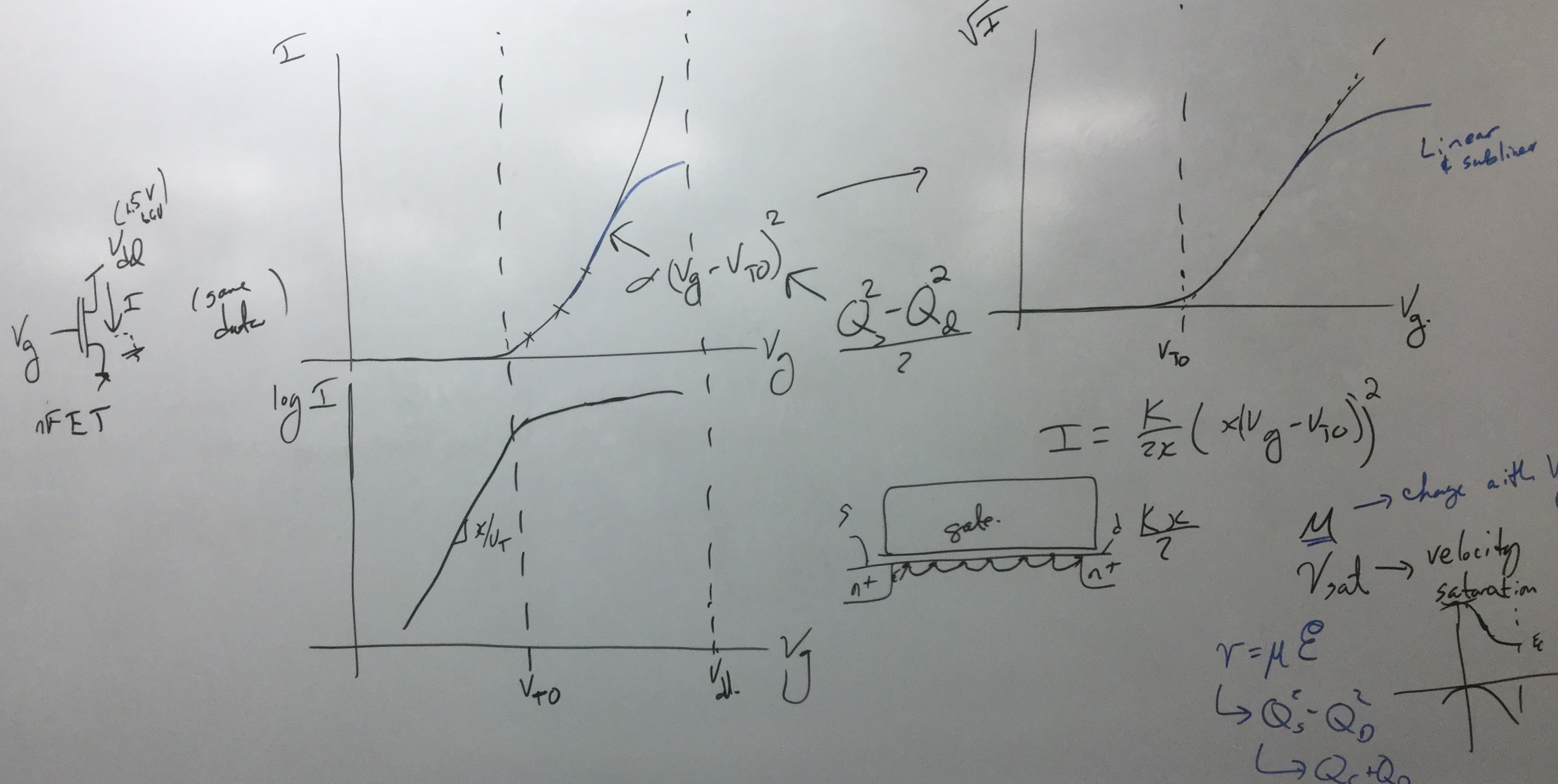
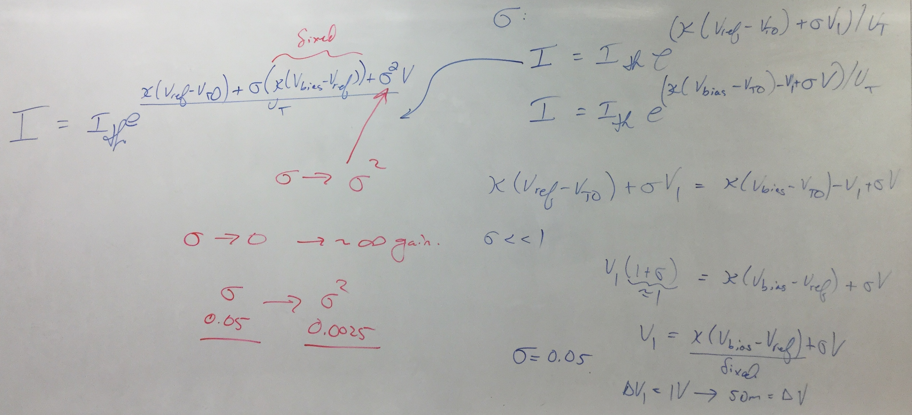
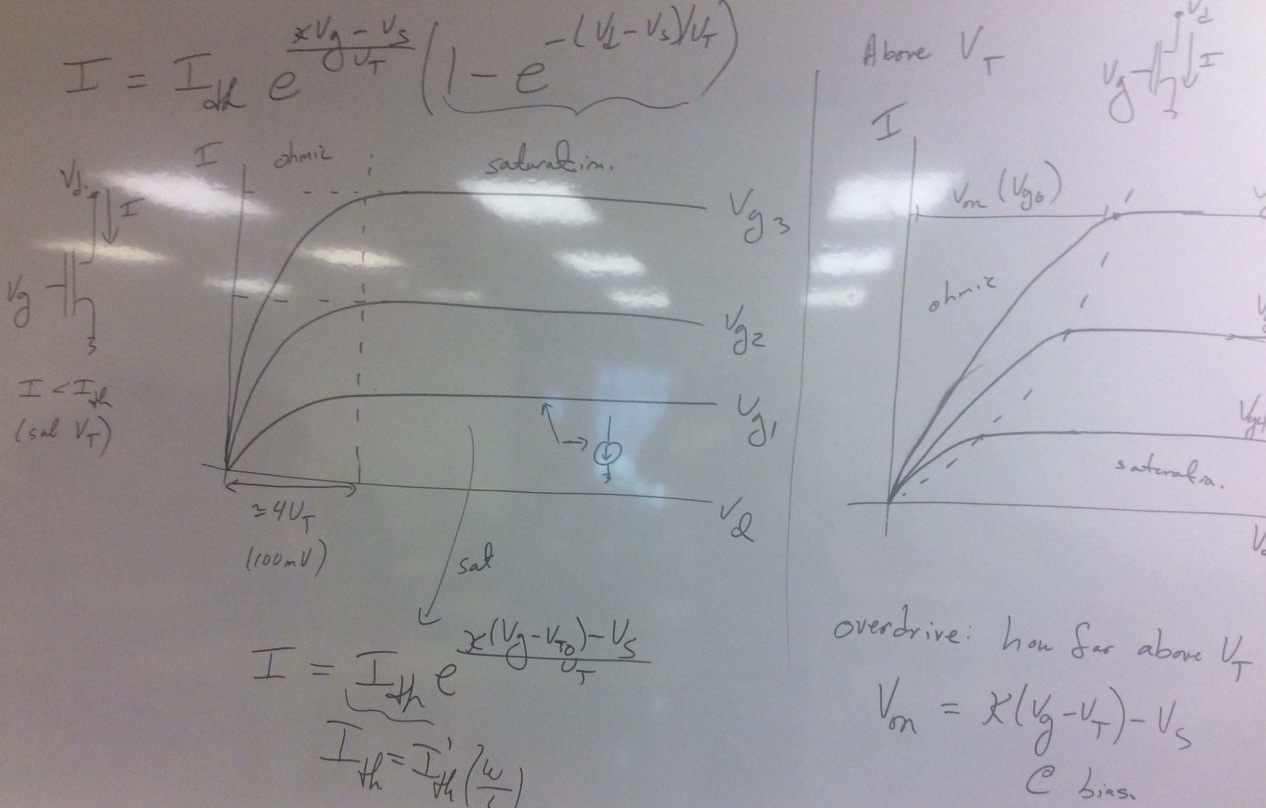
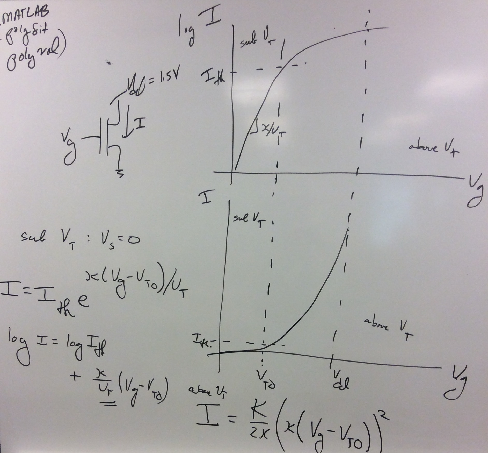
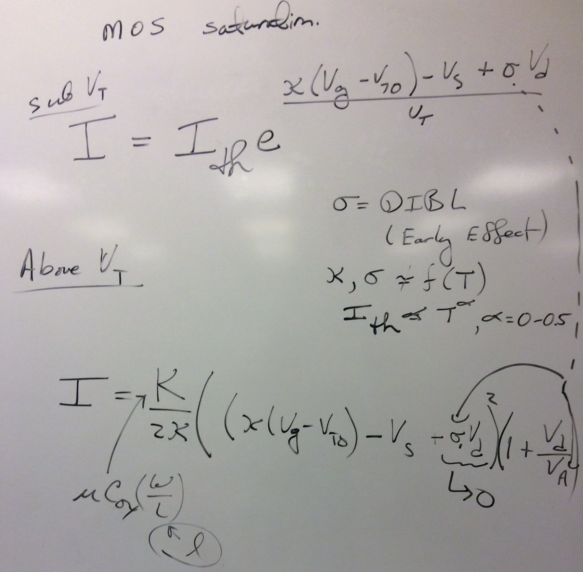
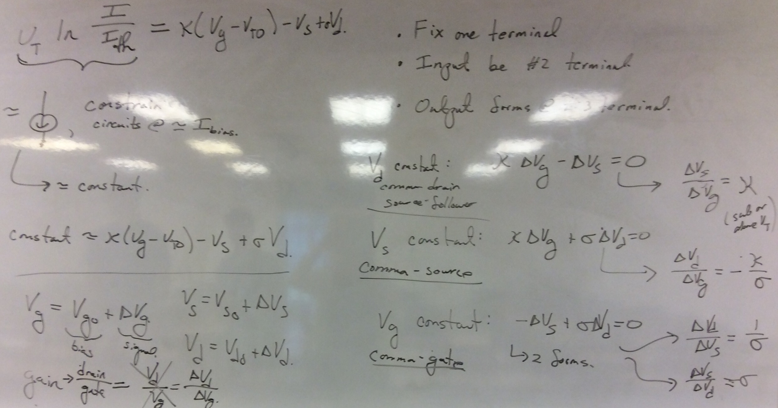
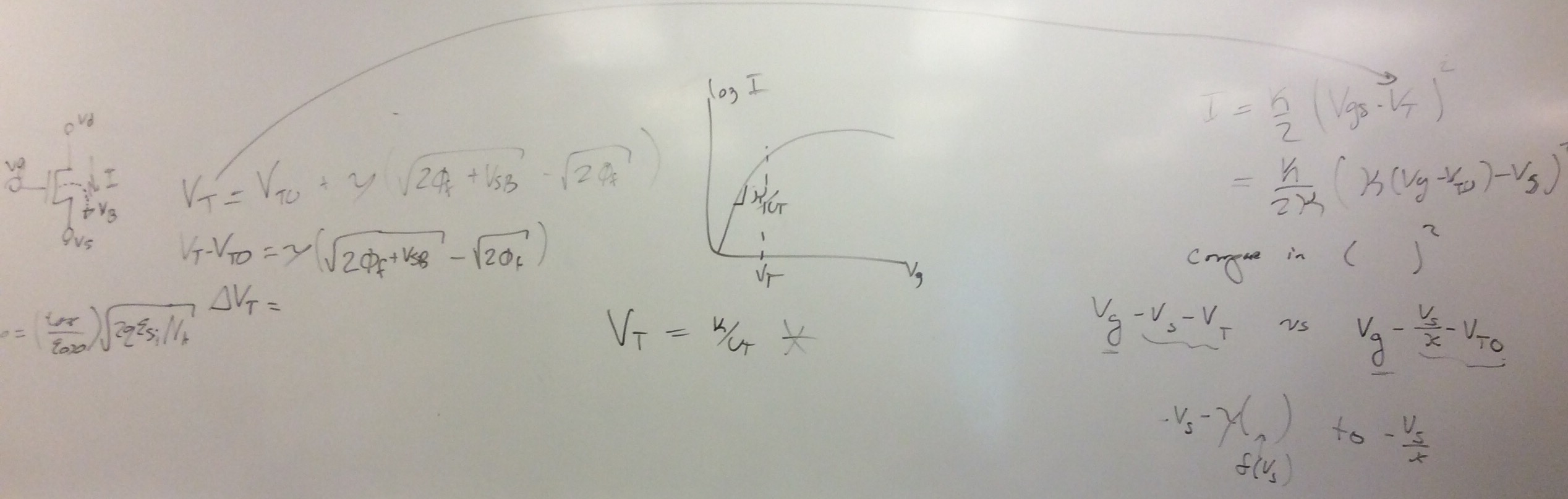
MOSFET I-V Physics ("sigma" = VA / U_T should be "sigma" = UT / V_A ) MOSFET I-V Physics 2 Qualitative AboveVT derivation, , | 1 2 3 4 5 | |
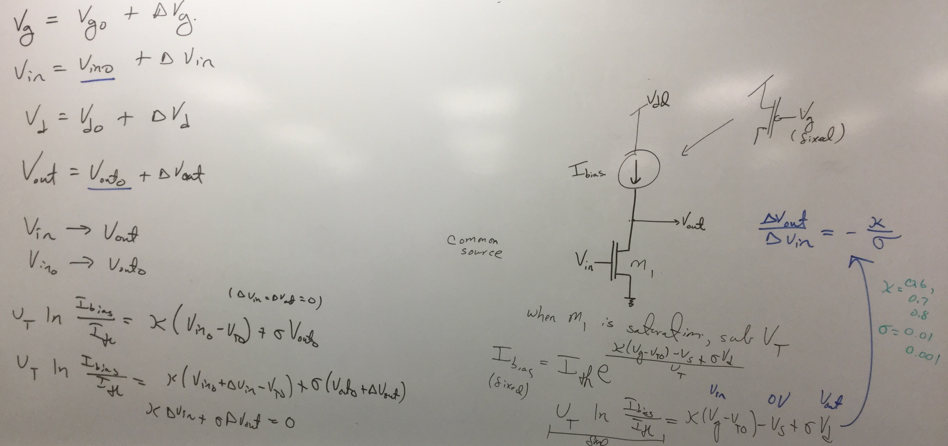
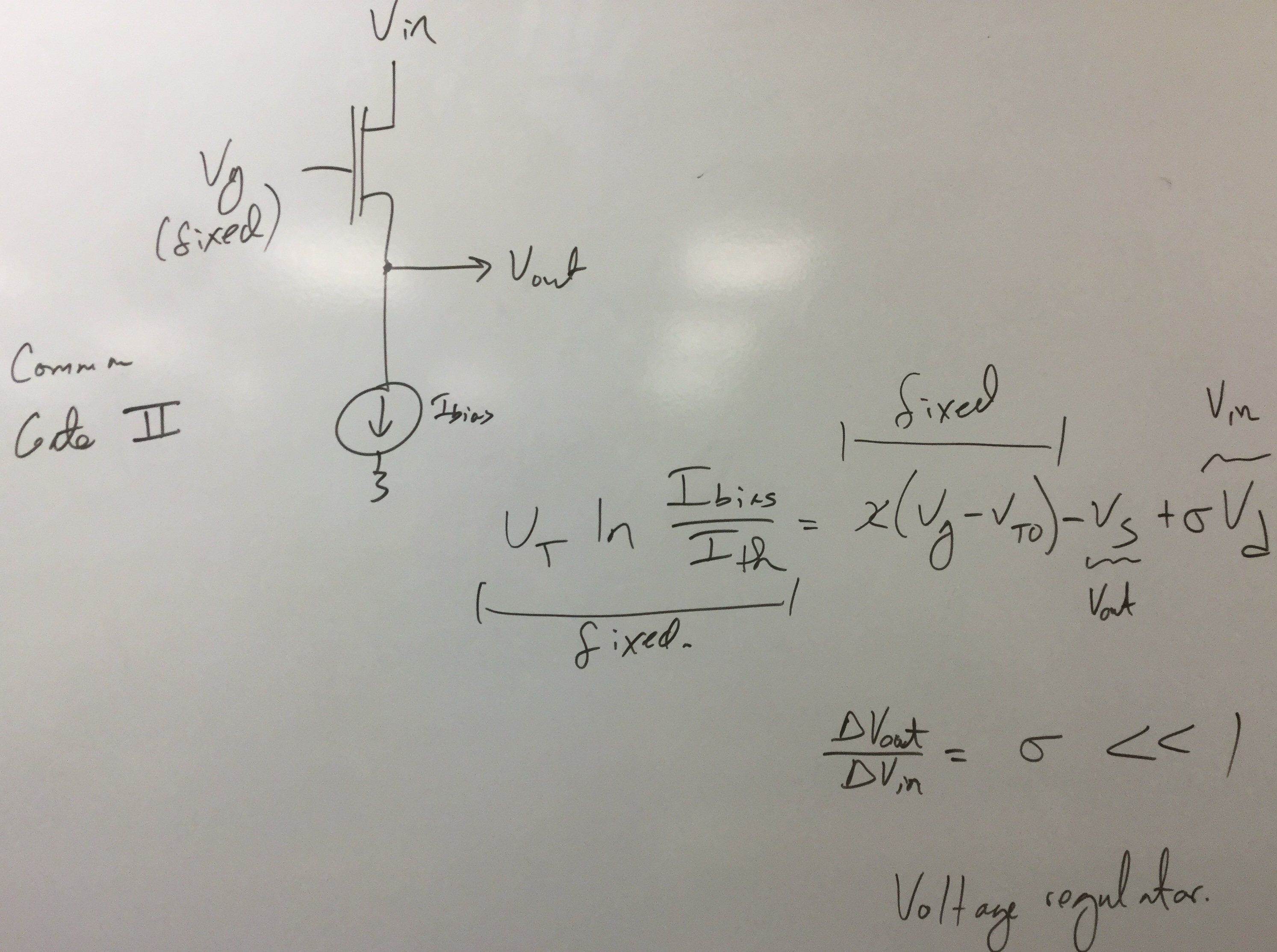
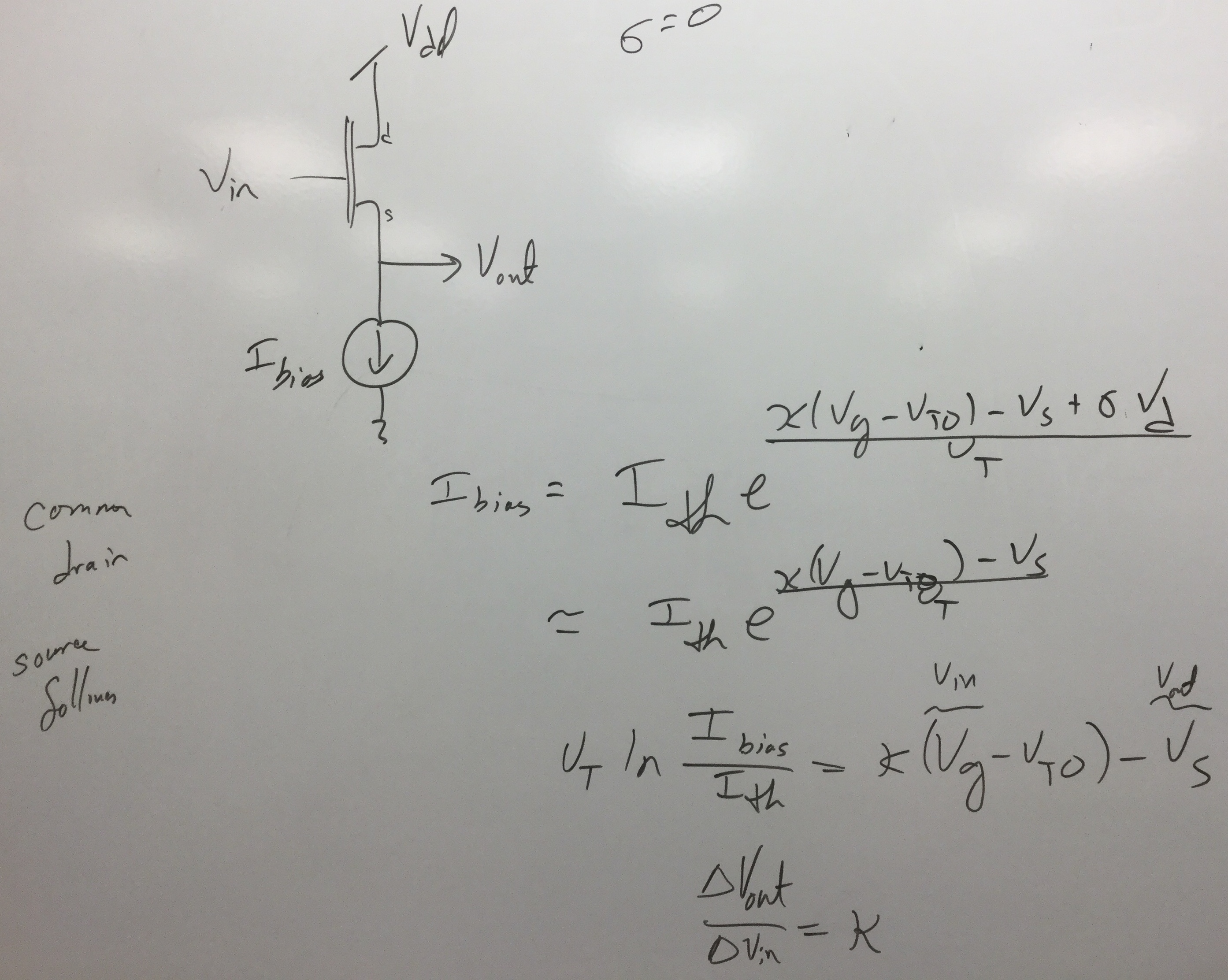
| Sept 1 | MOSFET II |
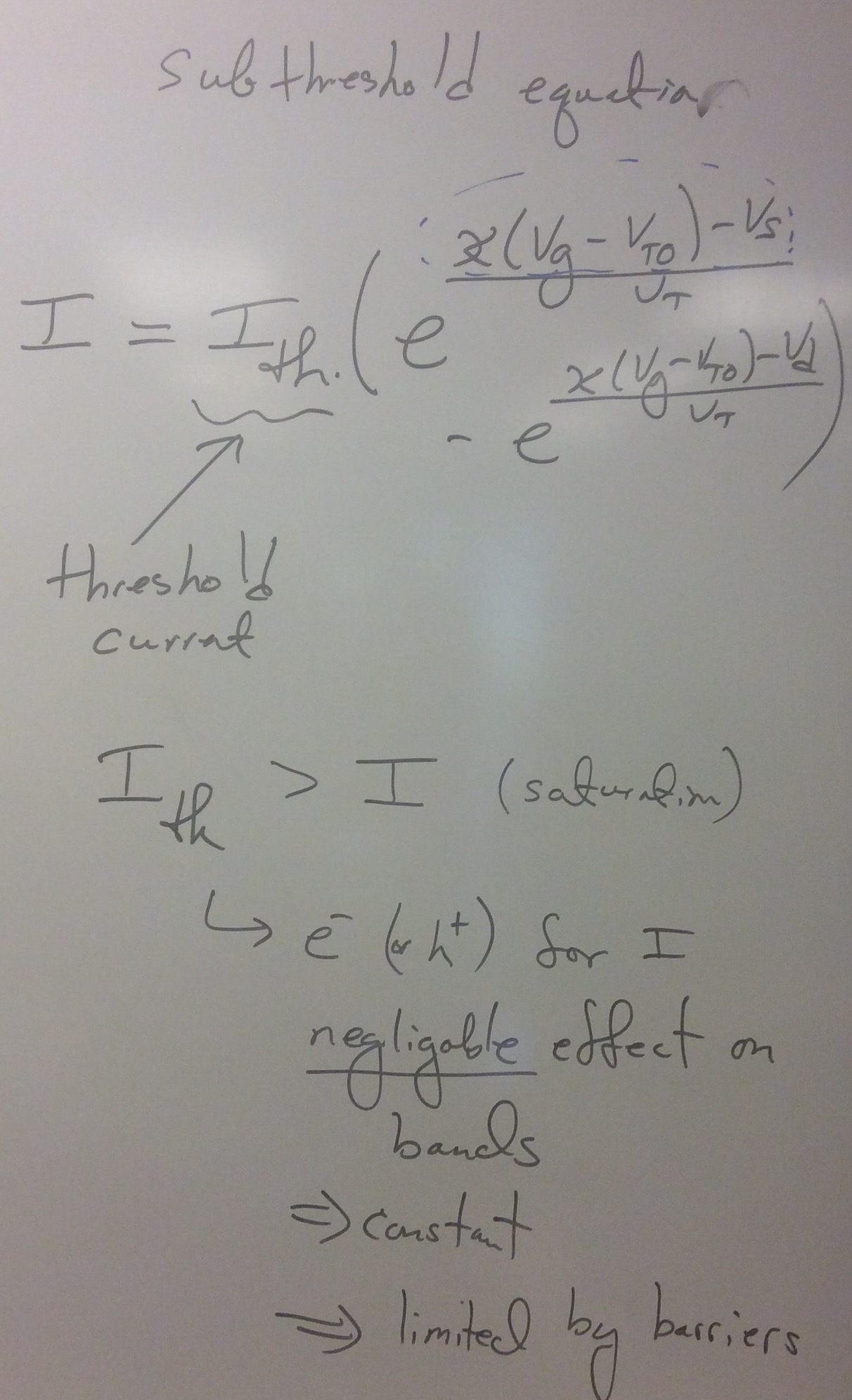
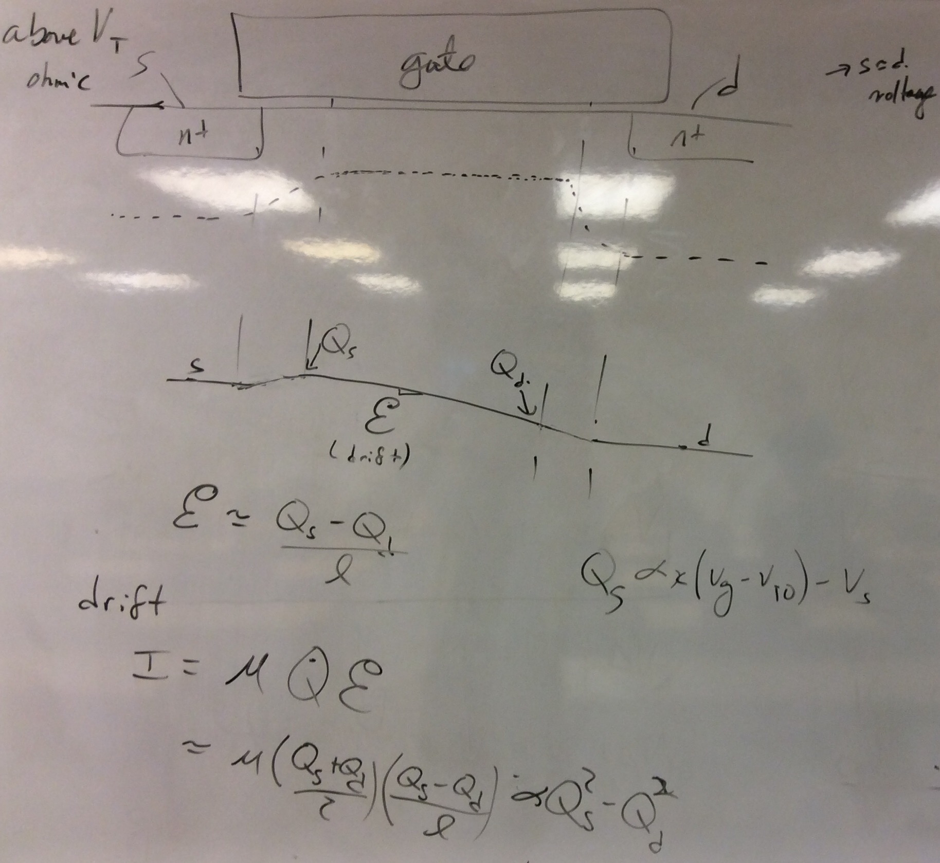
Subthreshold Derivation,
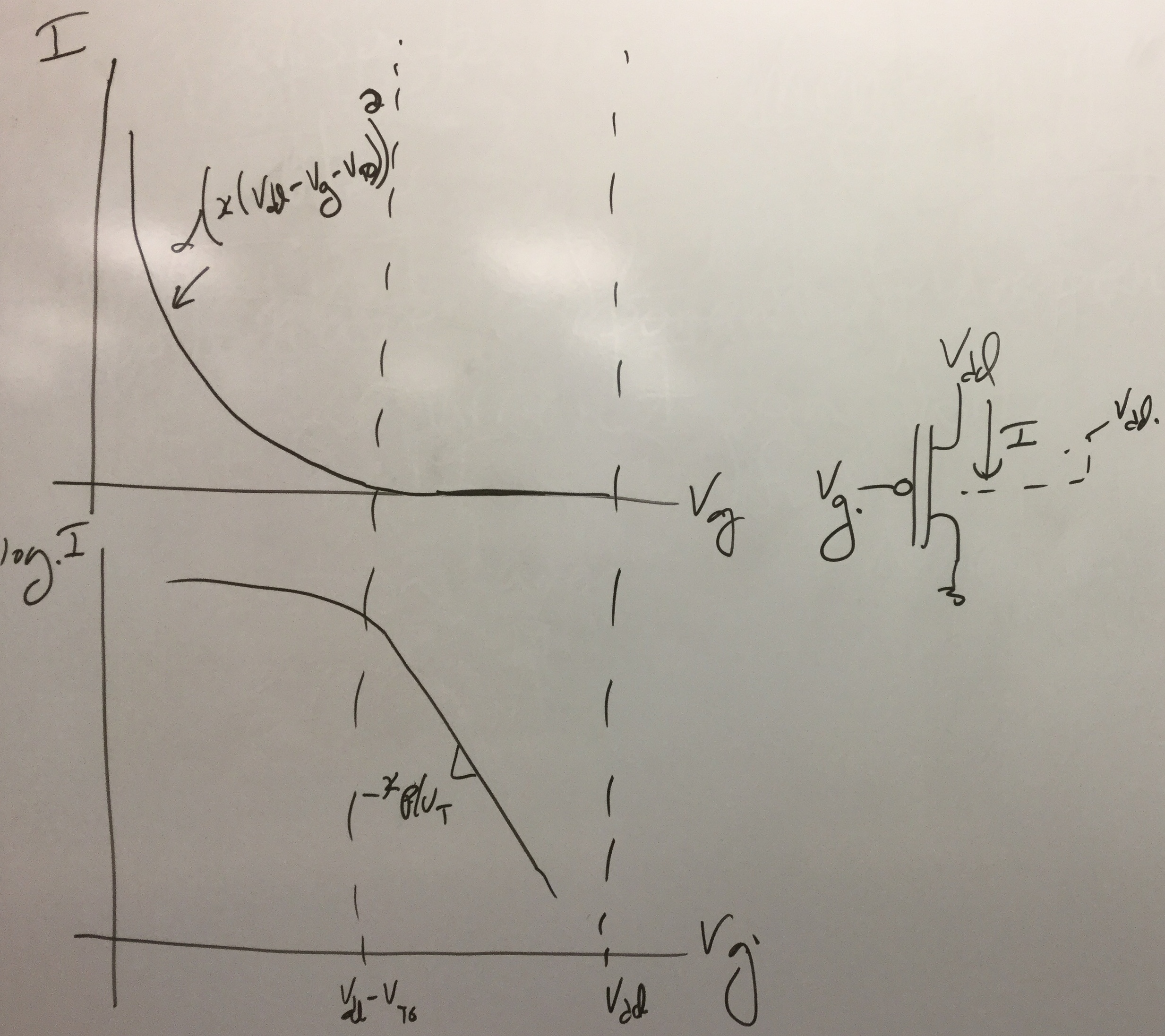
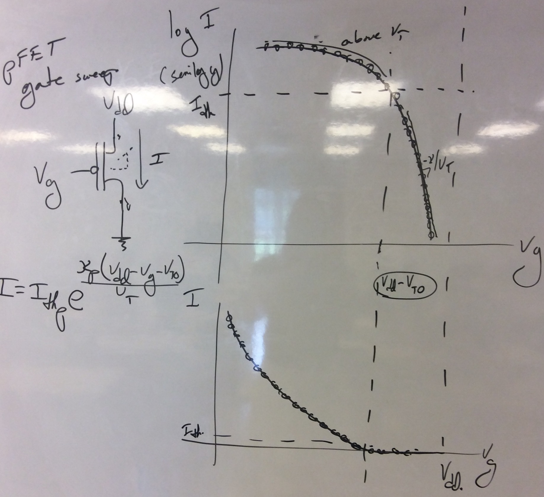
Above-Threshold derivation , A pFET I-V Device, A Tobi Element. , | Subthreshold Transistor Physics | 1, 2, 3, 4, |
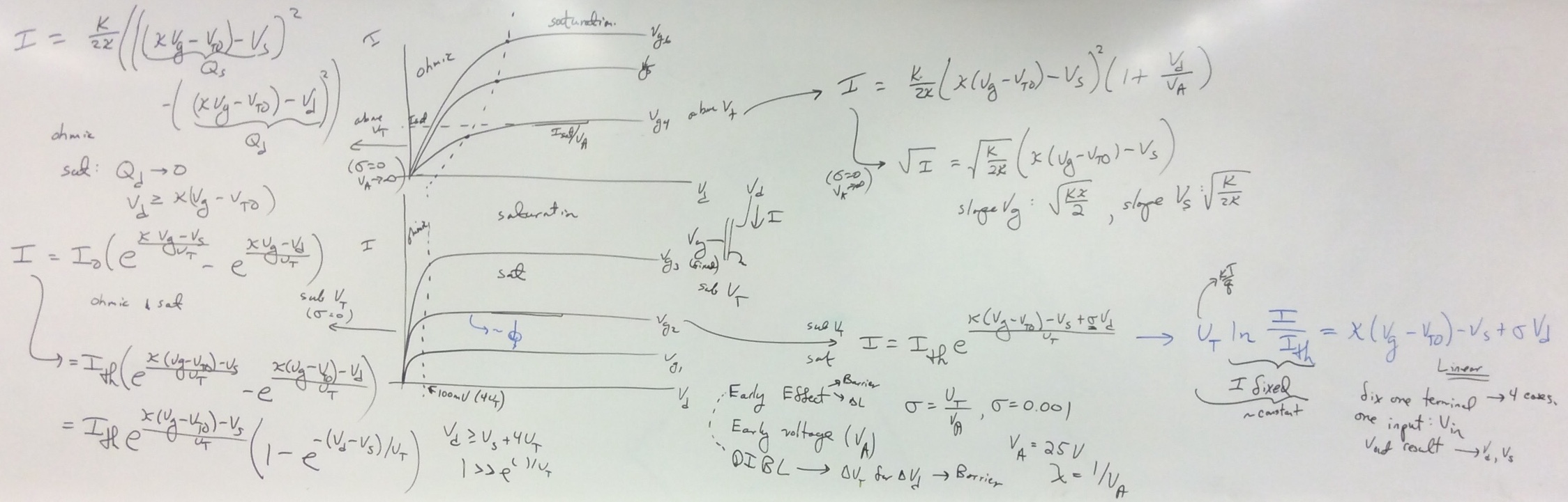
| Sept 3 | MOSFET Vd |
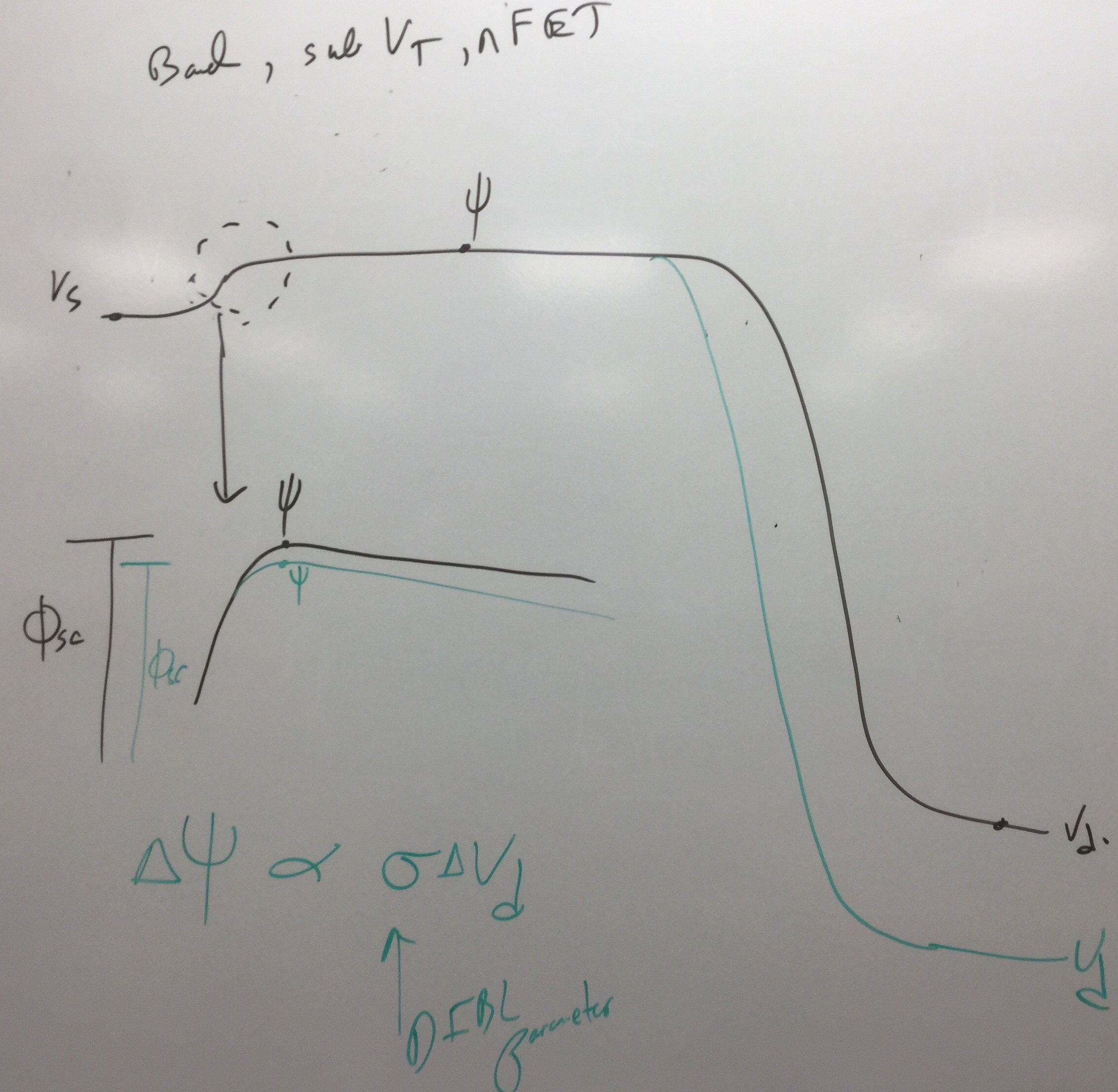
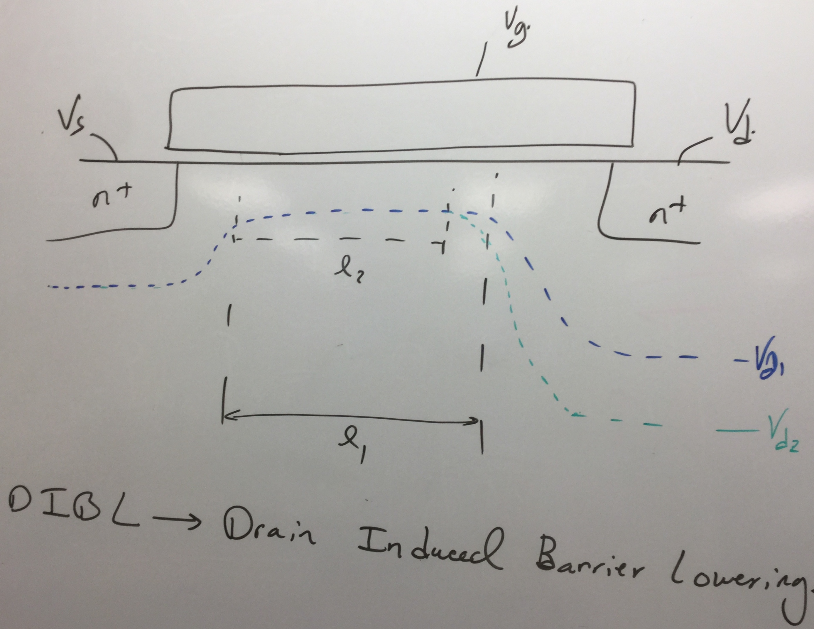
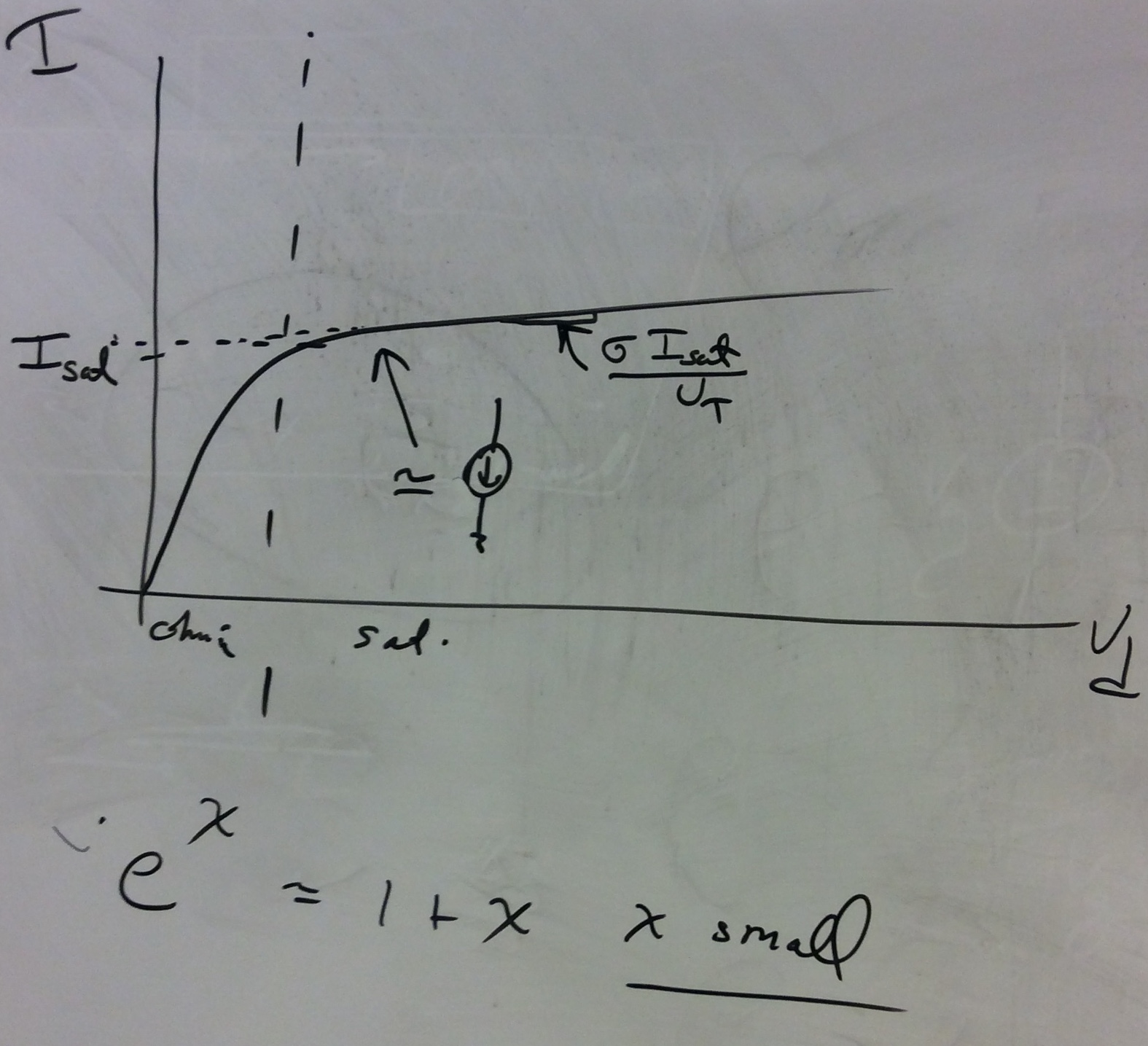
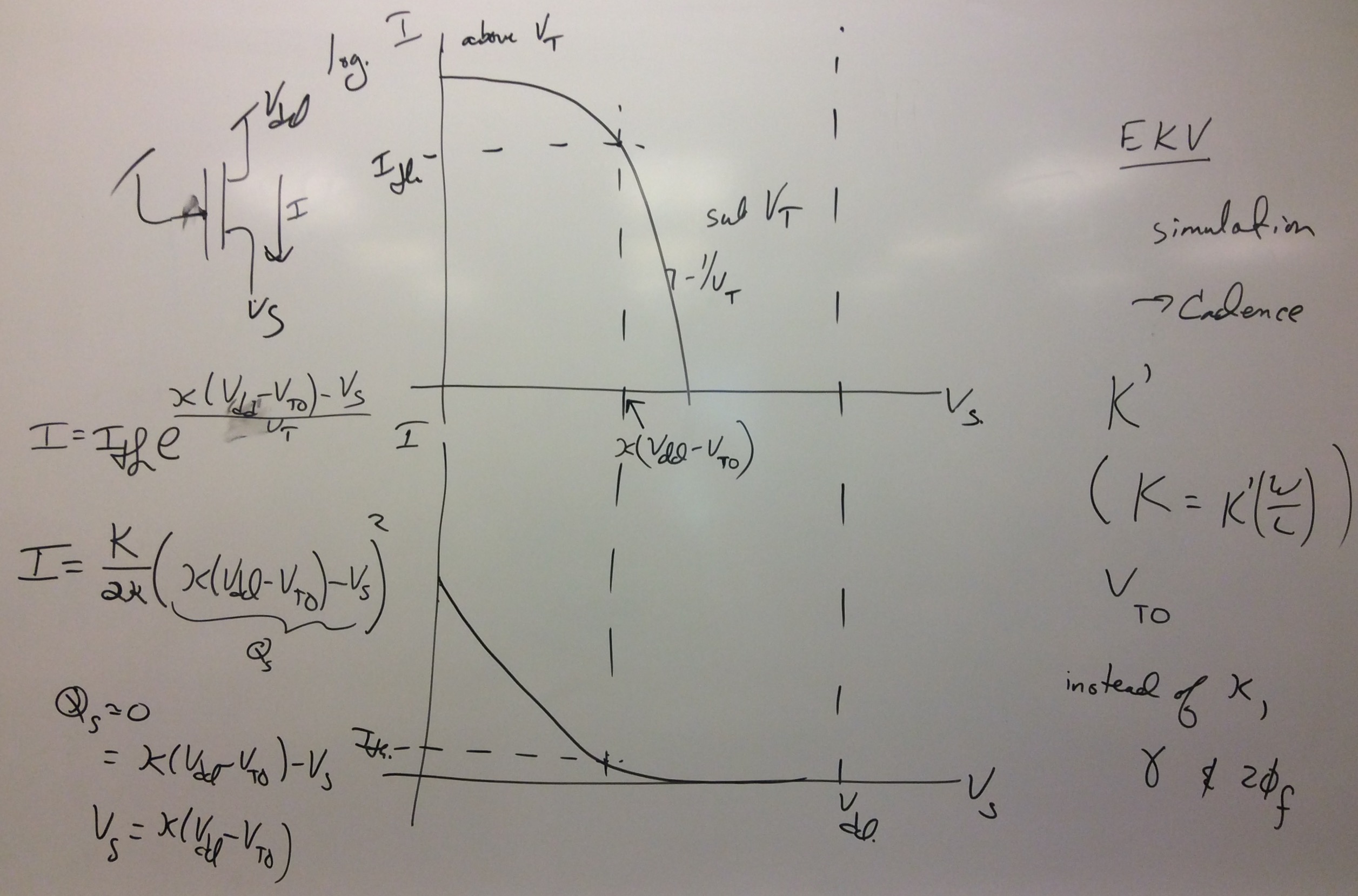
Early to Early Voltage
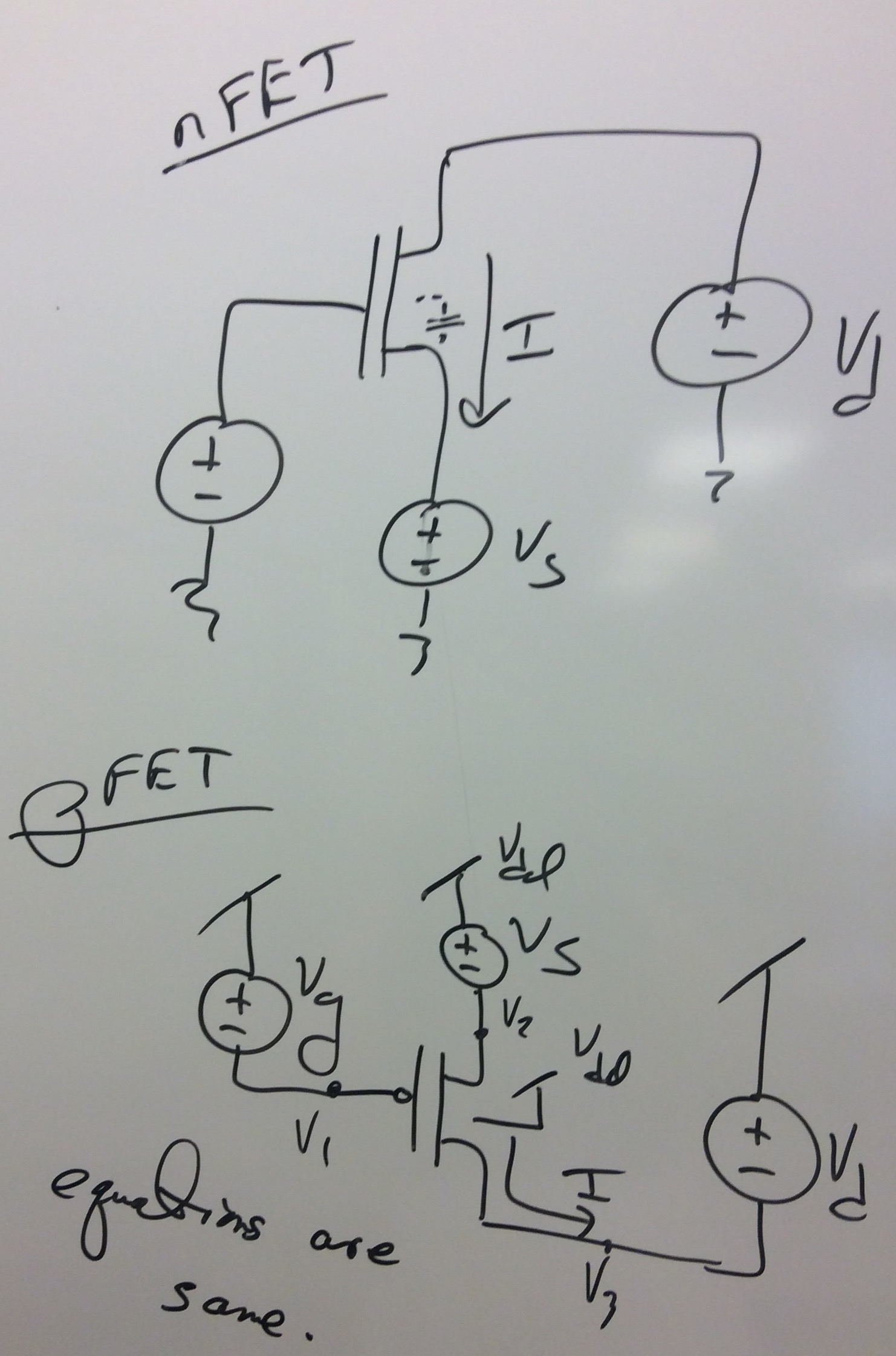
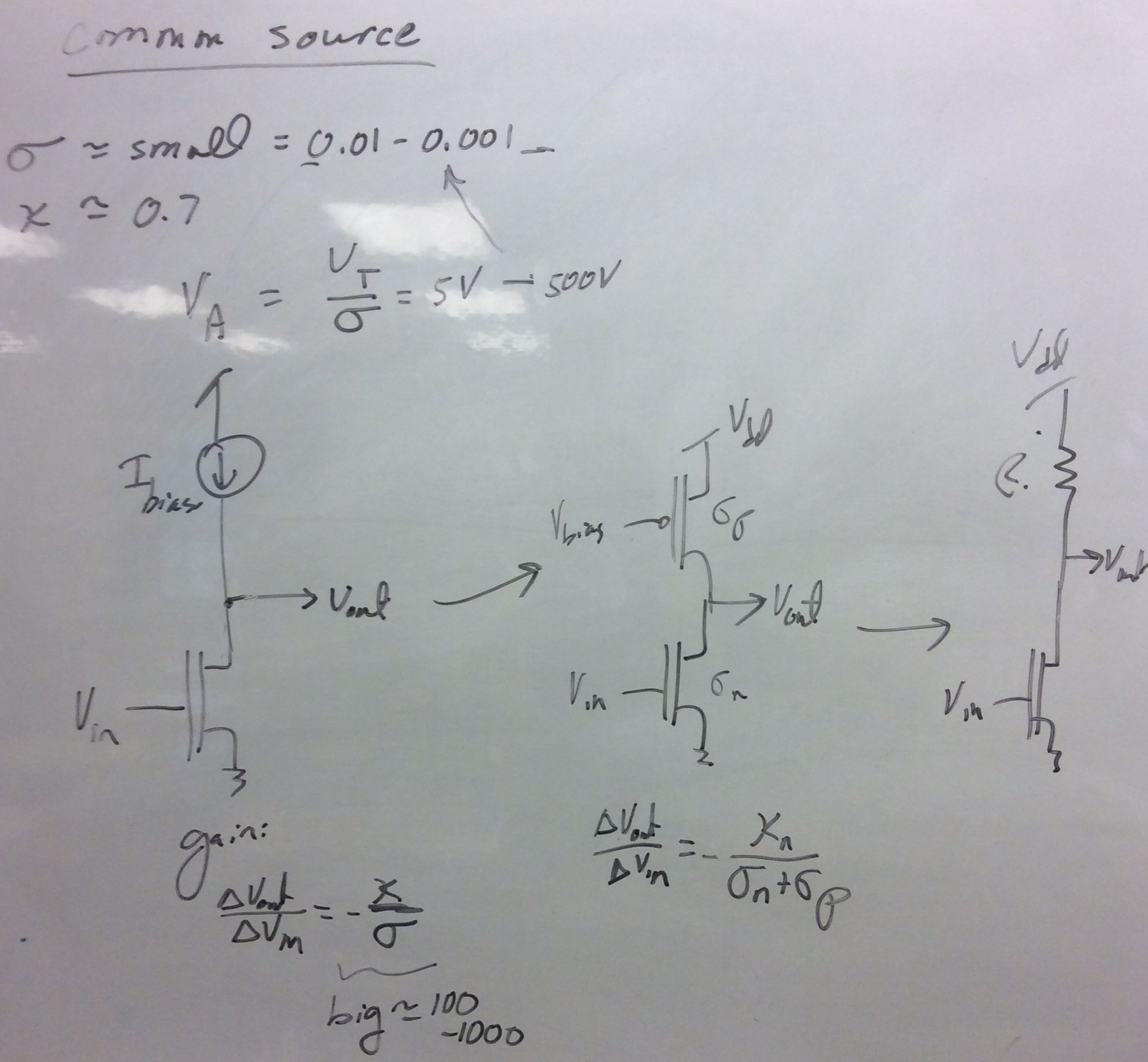
DIBL Modeling nFET sweep I pFET sweep II Two nFET configuration , | Classic DIBL paper / "sigma" | 1, 2, 3, 4, 5, 6, 7, 8, 9, |
| Sept 8 |
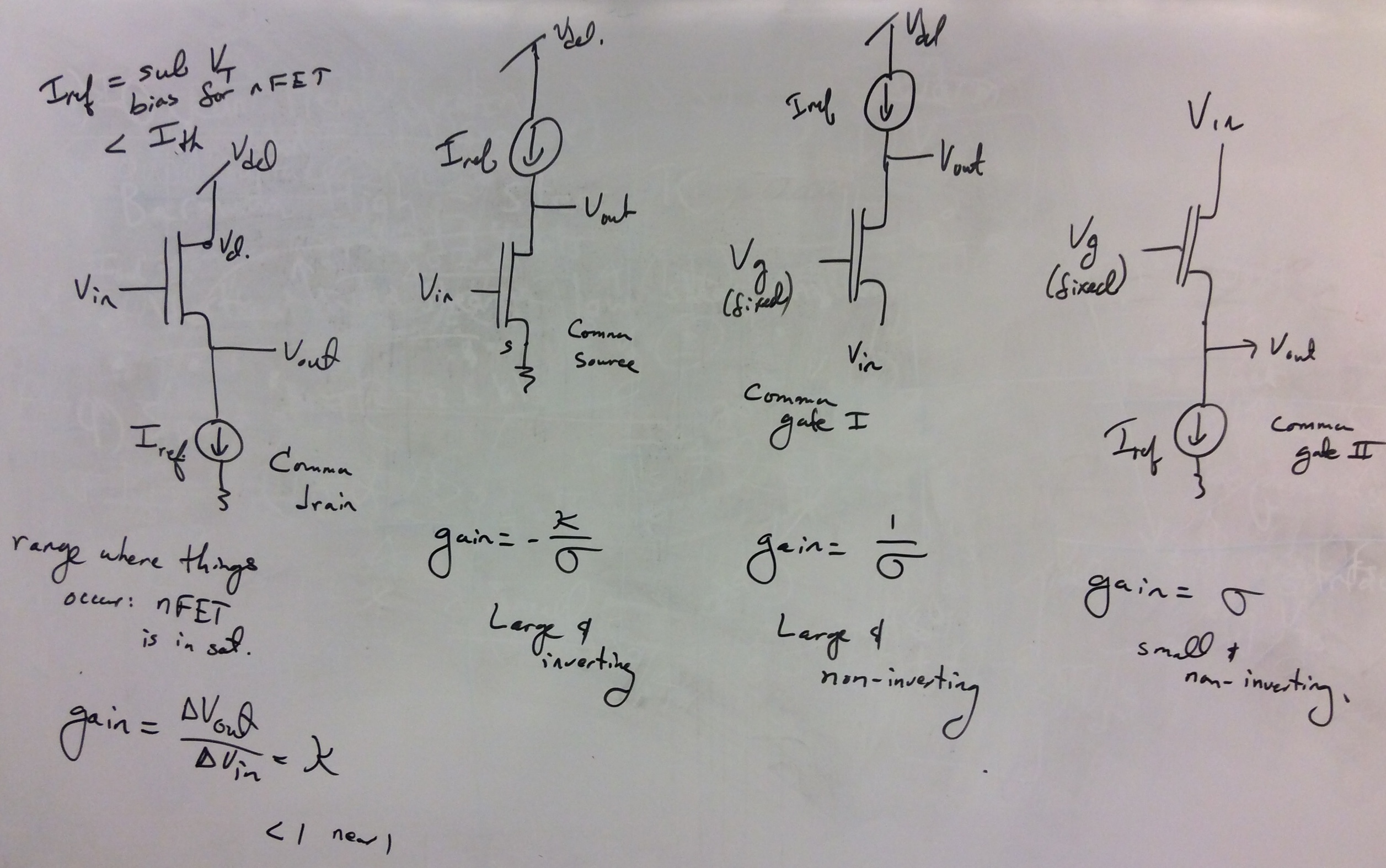
MOSFET = Current Source |
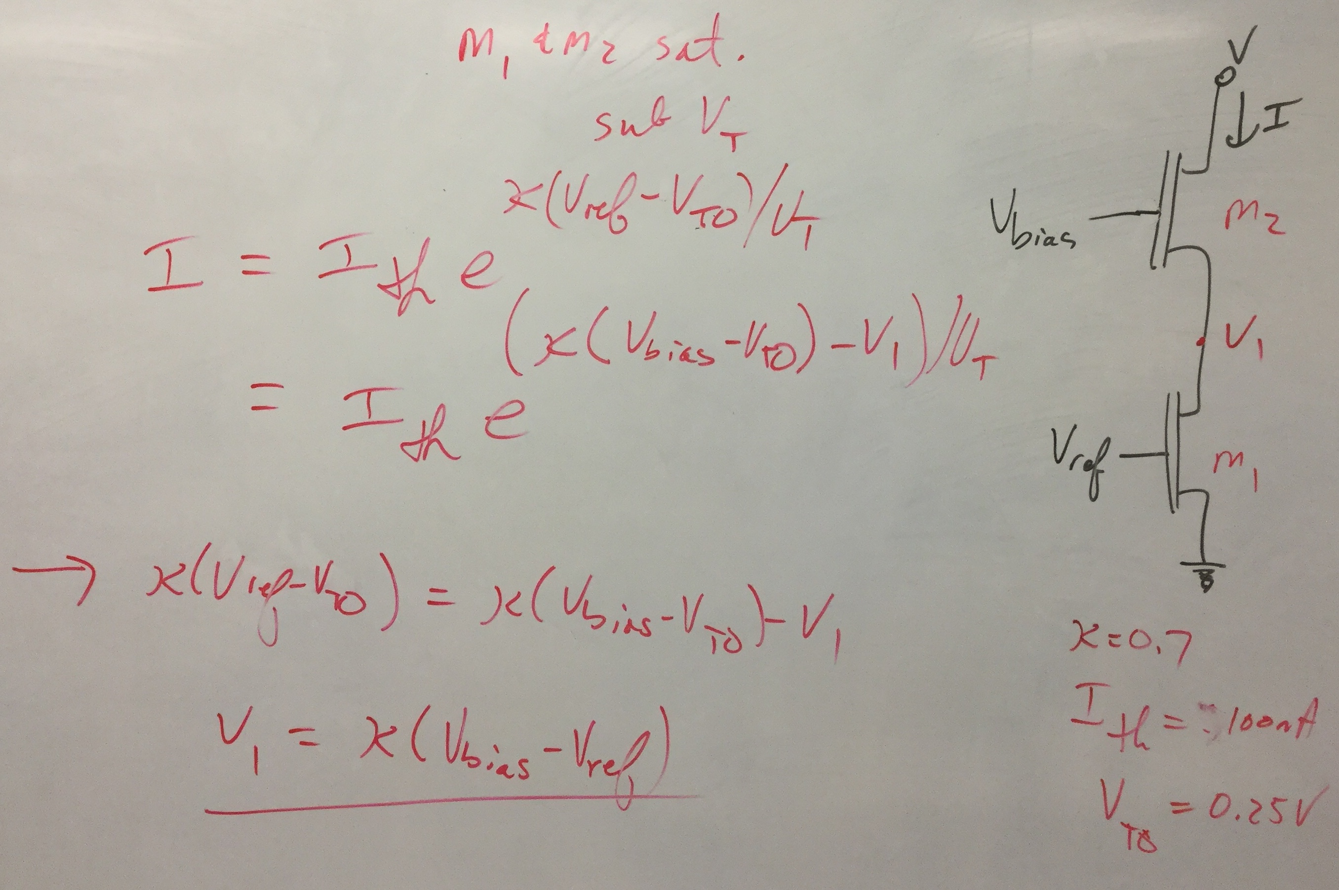
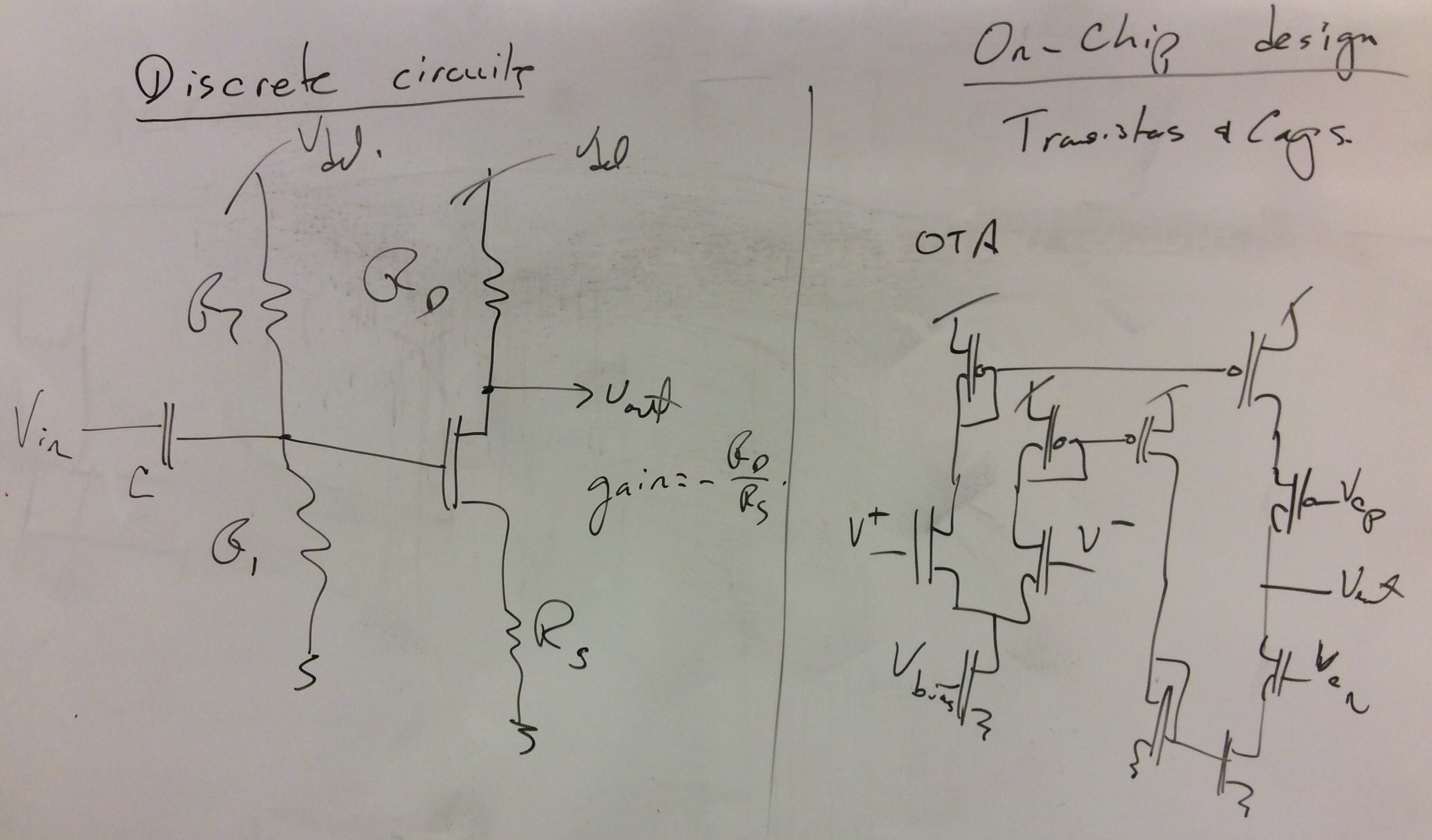
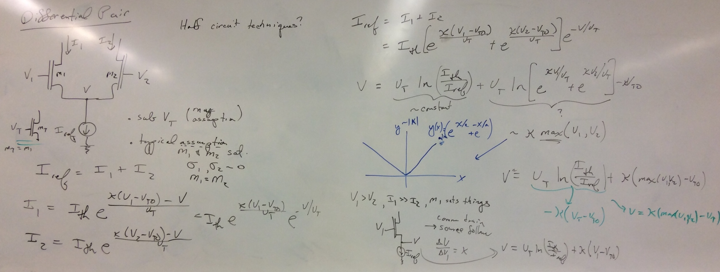
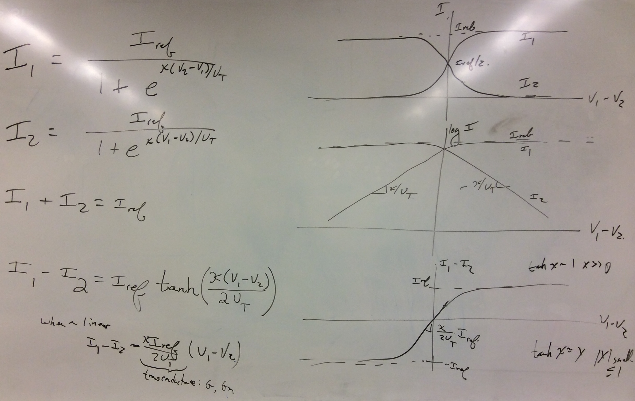
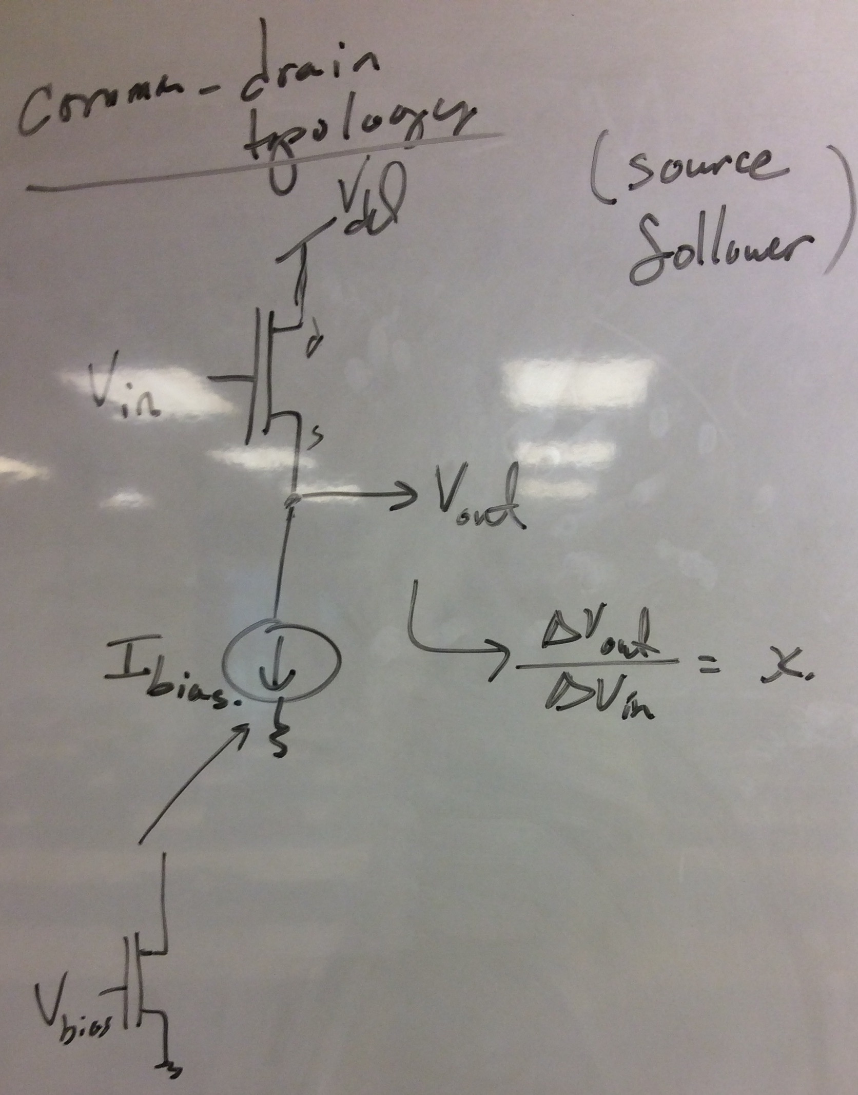
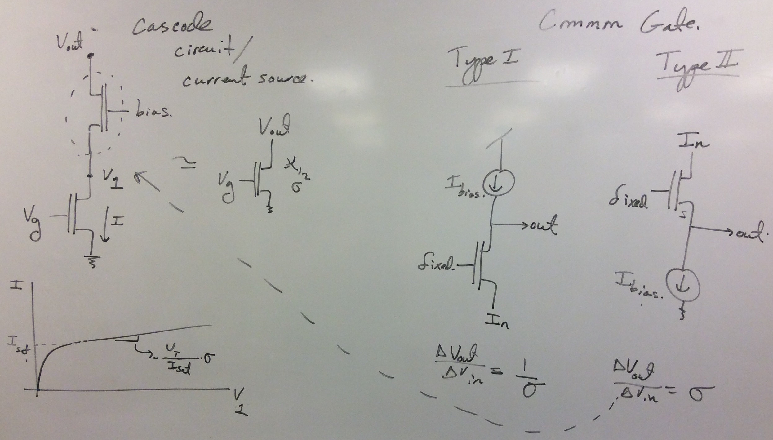
MOSFET = Current Source, Building Dependent Sources | 1, 2, 3, 4, 5, 6, | |
| Sept 10 | Project Review |
Project Due Sept 10 (11:59pm ATL time)
Tentitive Gradiing
Rubric
(any part can change at any time).
A few critical points to remember:
Lectures from Dr. Brad Minch (Olin) tht might be helpful:
Lectures from Ali Hajimiri (Caltech) that might be helpful:
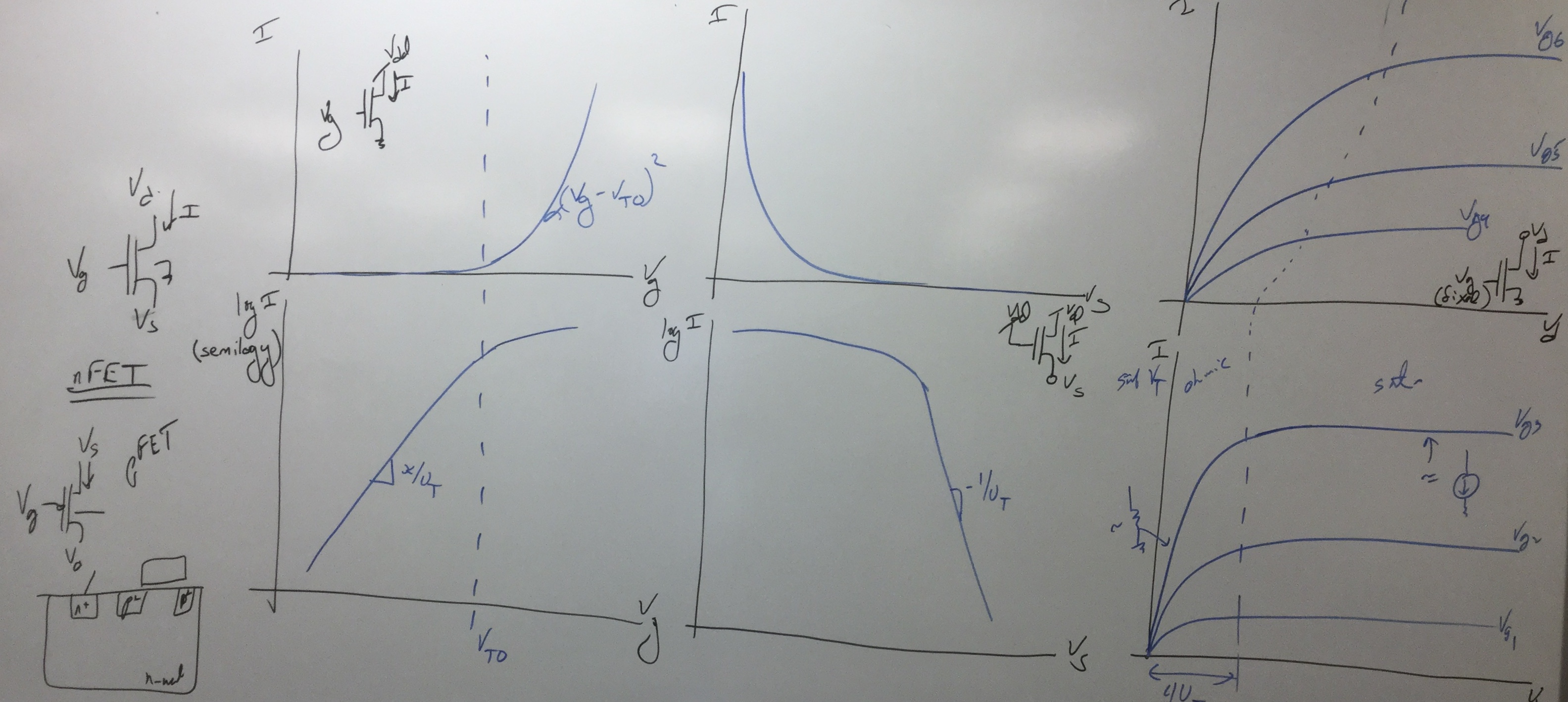
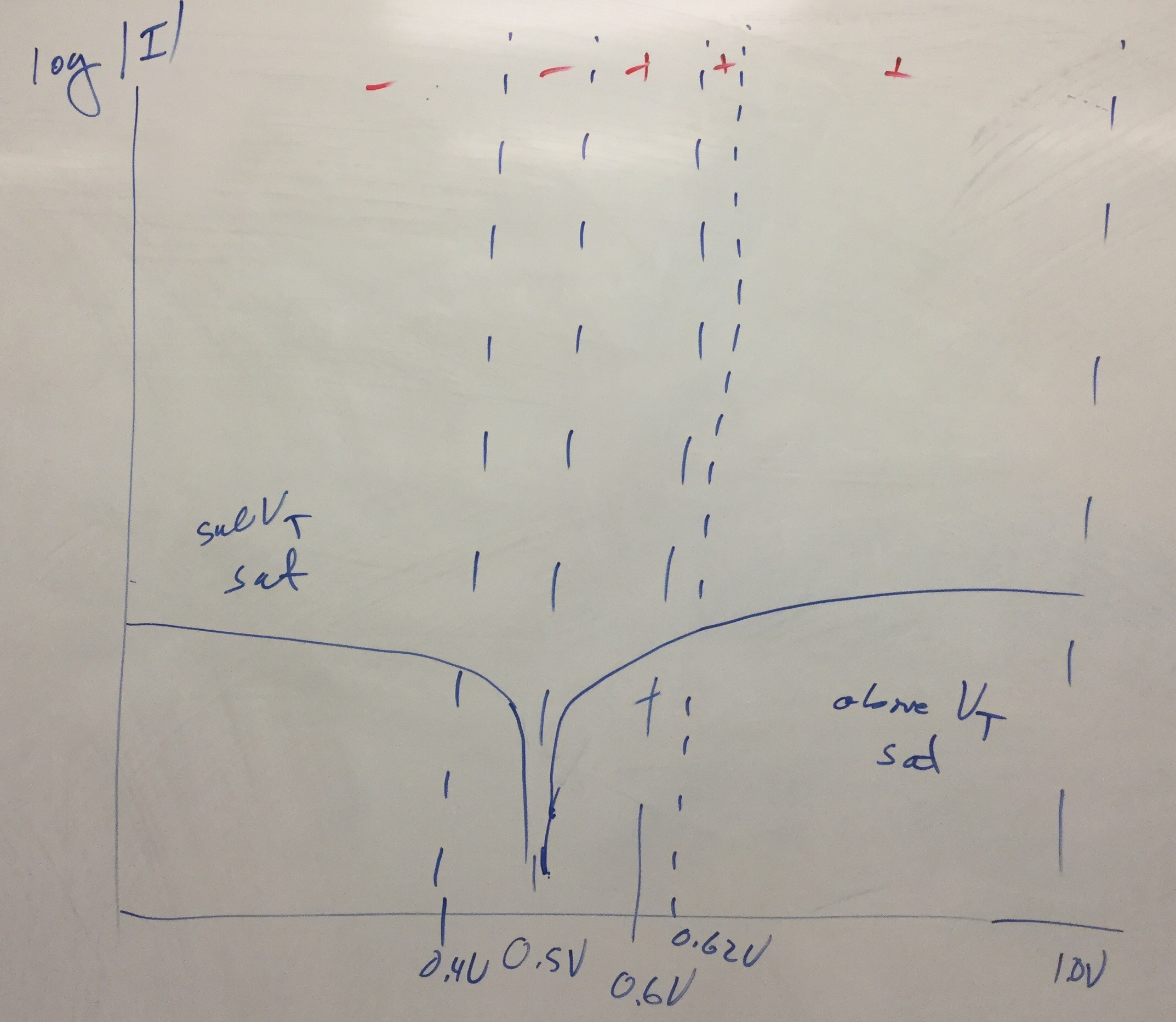
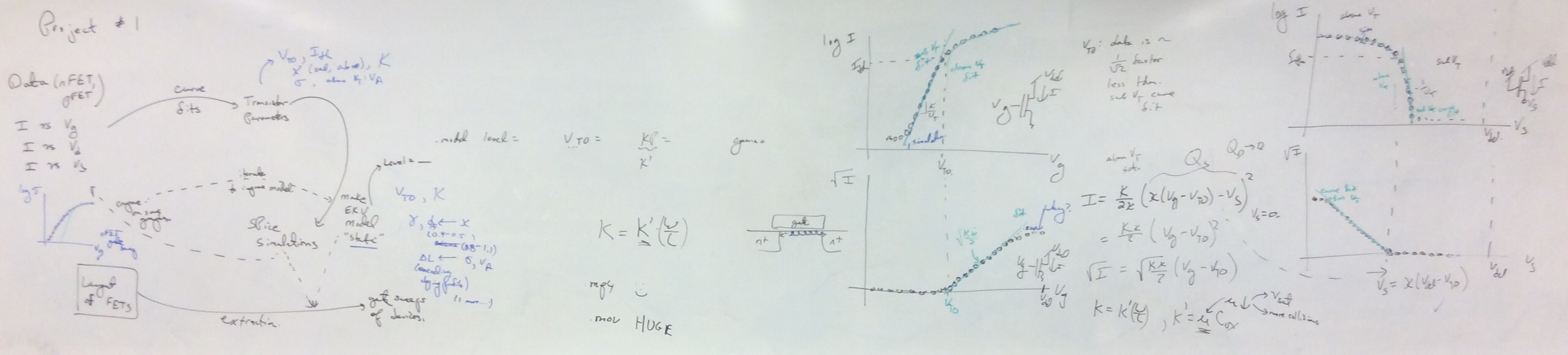
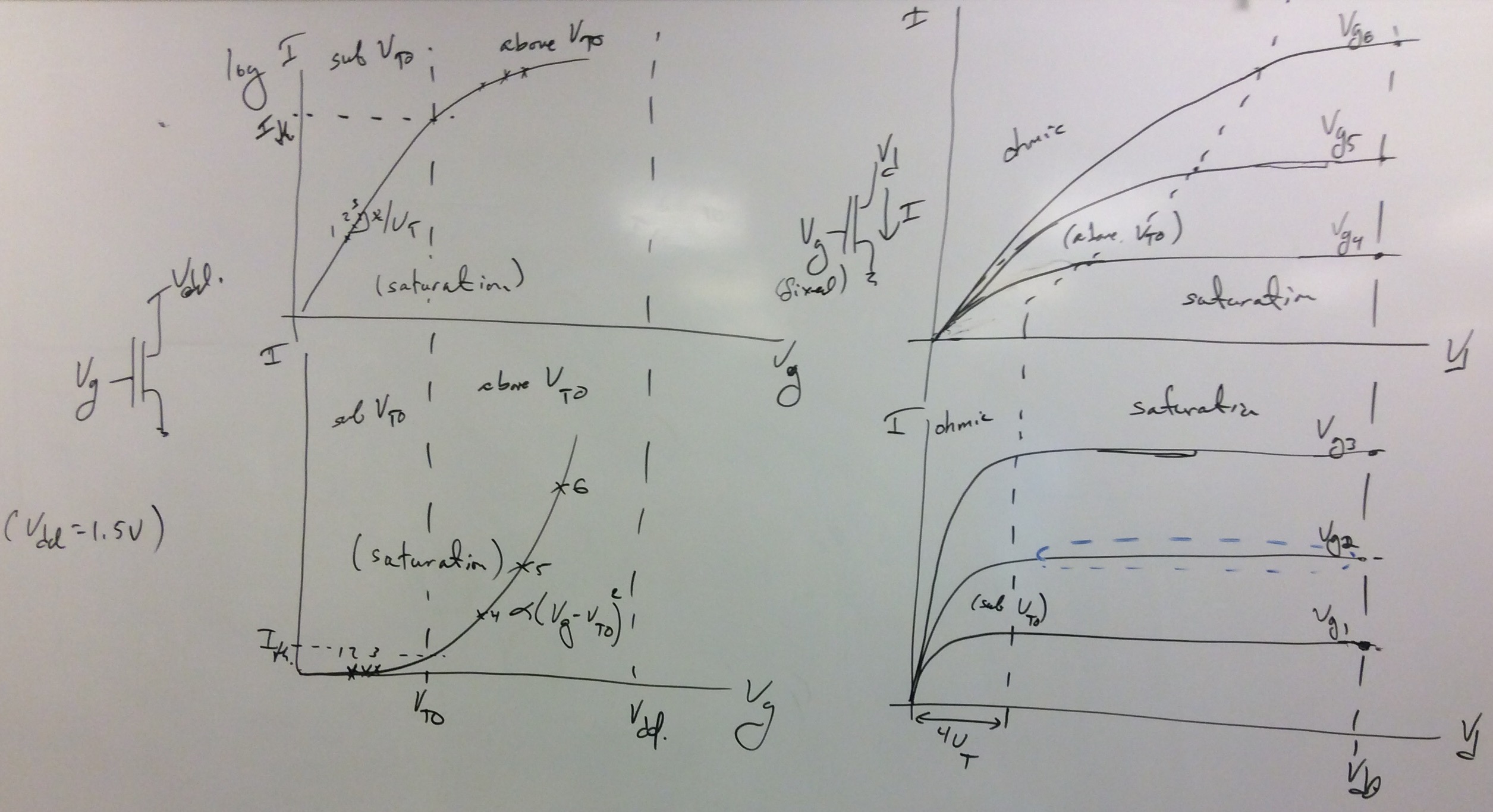
You will use the provided Skywater 130nm CMOS measurement of source current versus gate voltage swept for a device with the source voltage held at GND / Vdd (nFET / pFET) for the device operating in saturation throughout the sweep (Vdd / GND for nFET / pFET ), as well as the device operating in ohmic regime for the device operating in saturation throughout the sweep (GND+10mV/Vdd=10mV for nFET / pFET ),
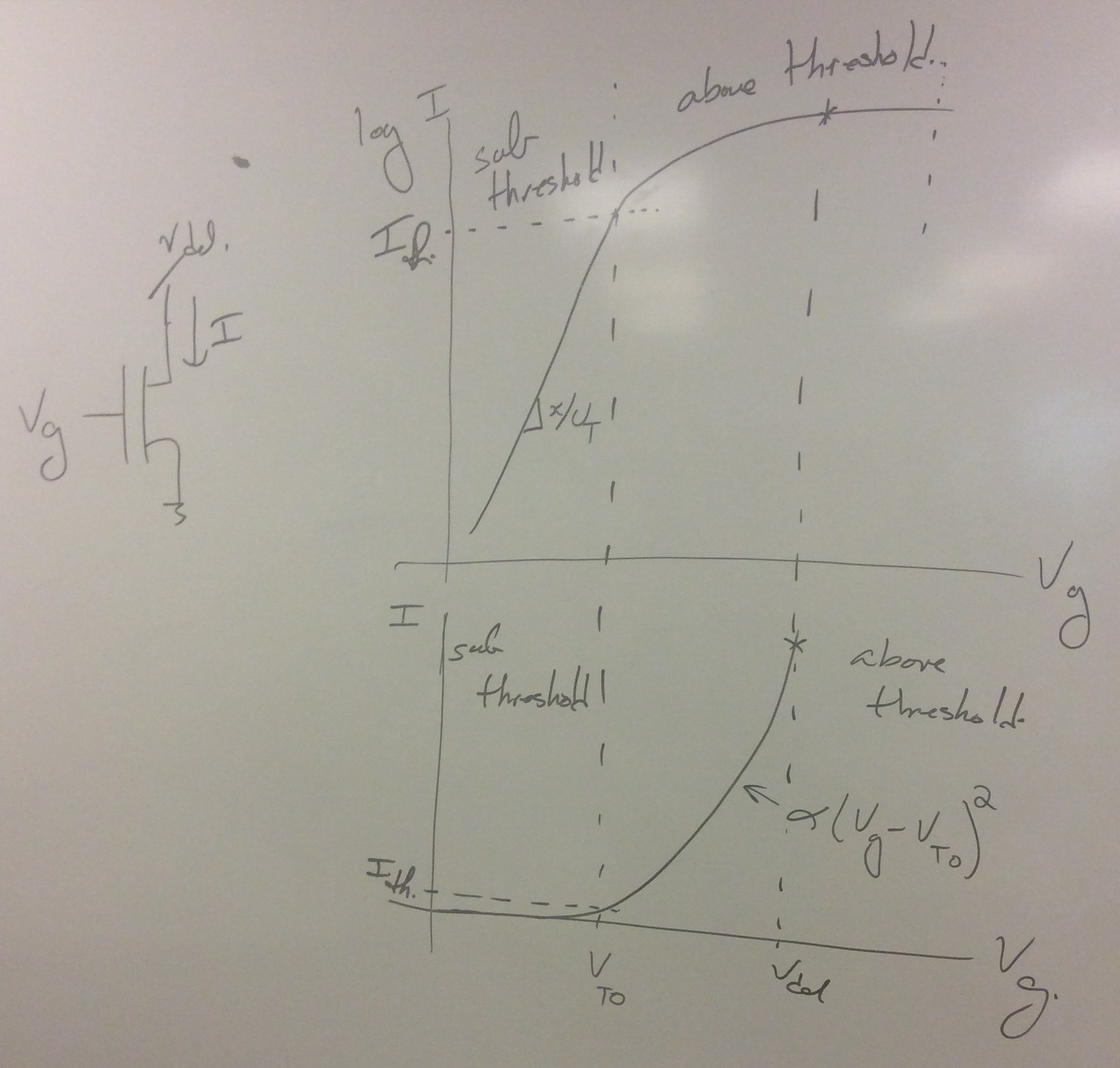
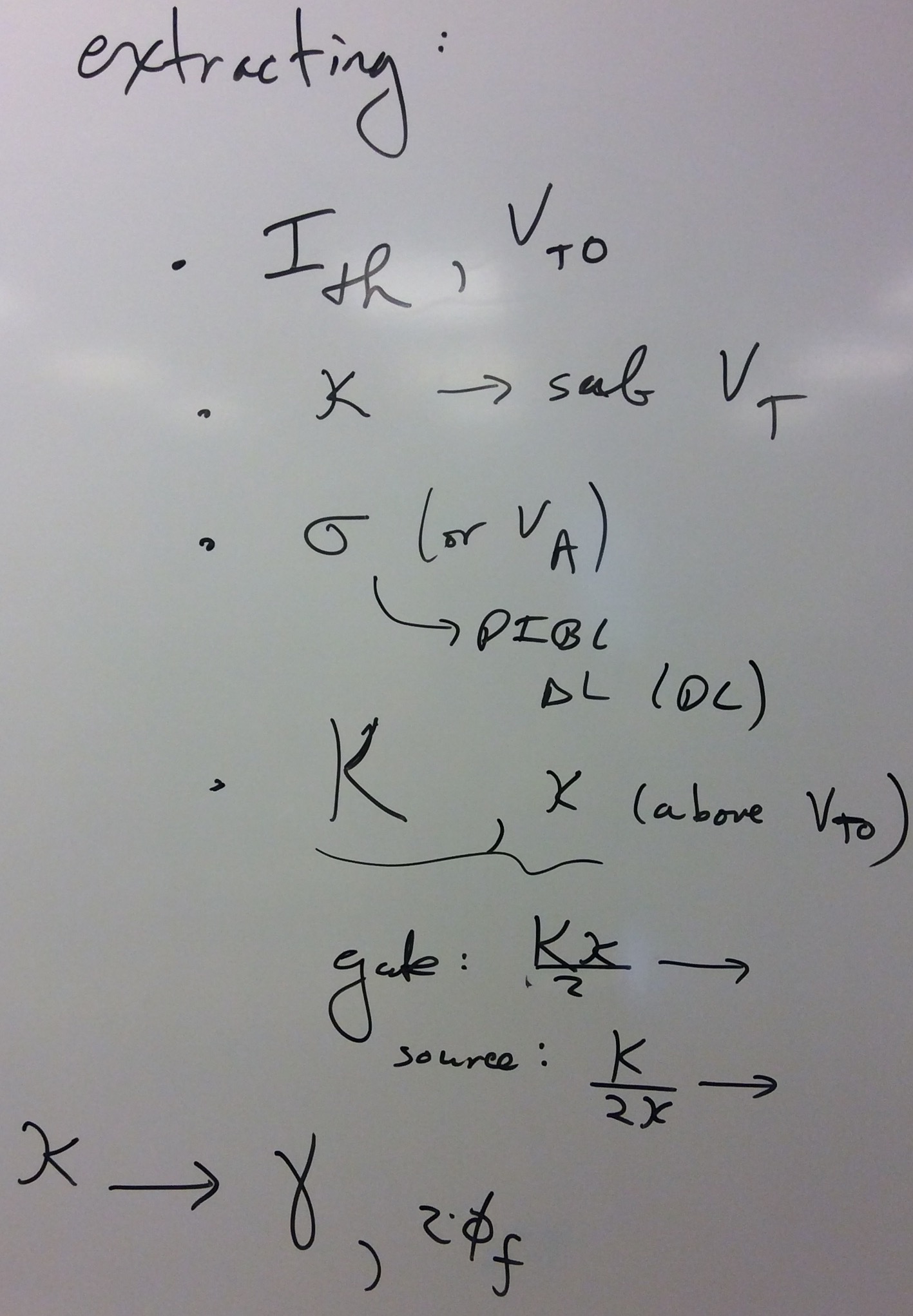
1. Fit the theoretical expression in the subthreshold saturation region of operation (an exponential curve fit) for the nFET and pFET curves. Identify "kappa" and threshold voltage and Io. Identify any interesting / unexpected parts of the graph, and explain where it comes from (i.e. do not say it was "measurement error"... what type of measurement error, if that is the case).
2. Fit the theoretical expression in the subthreshold ohmic
(|Vd-V
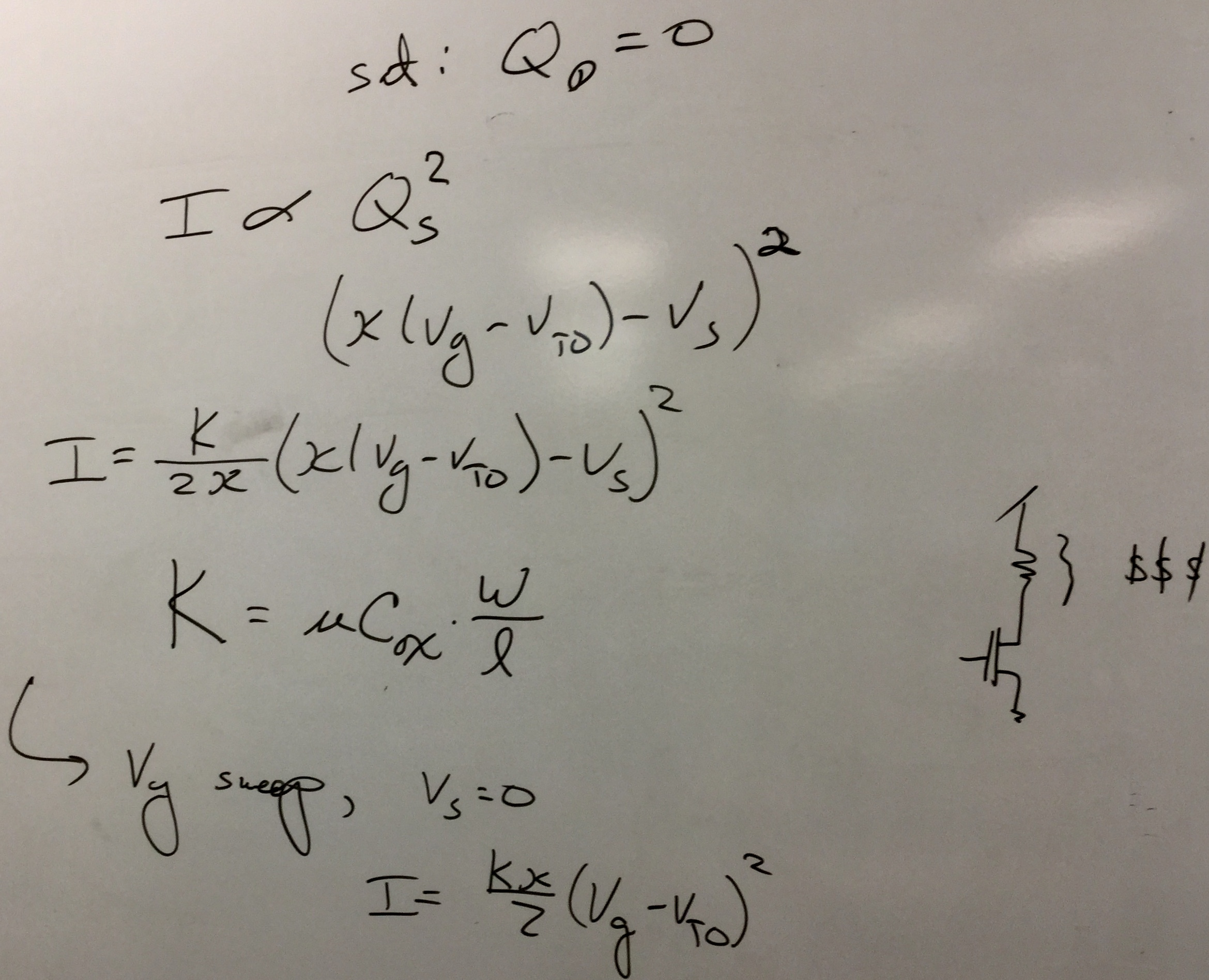
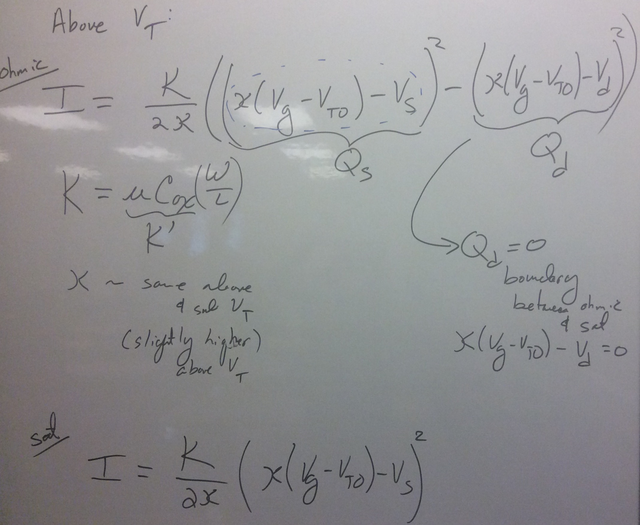
3. Fit the theoretical expression in the above-threshold ohmic region of operation (a linear) curve fit) for the nFET and pFET curves. Identify K and VT0. Identify any interesting / unexpected parts of the graph.
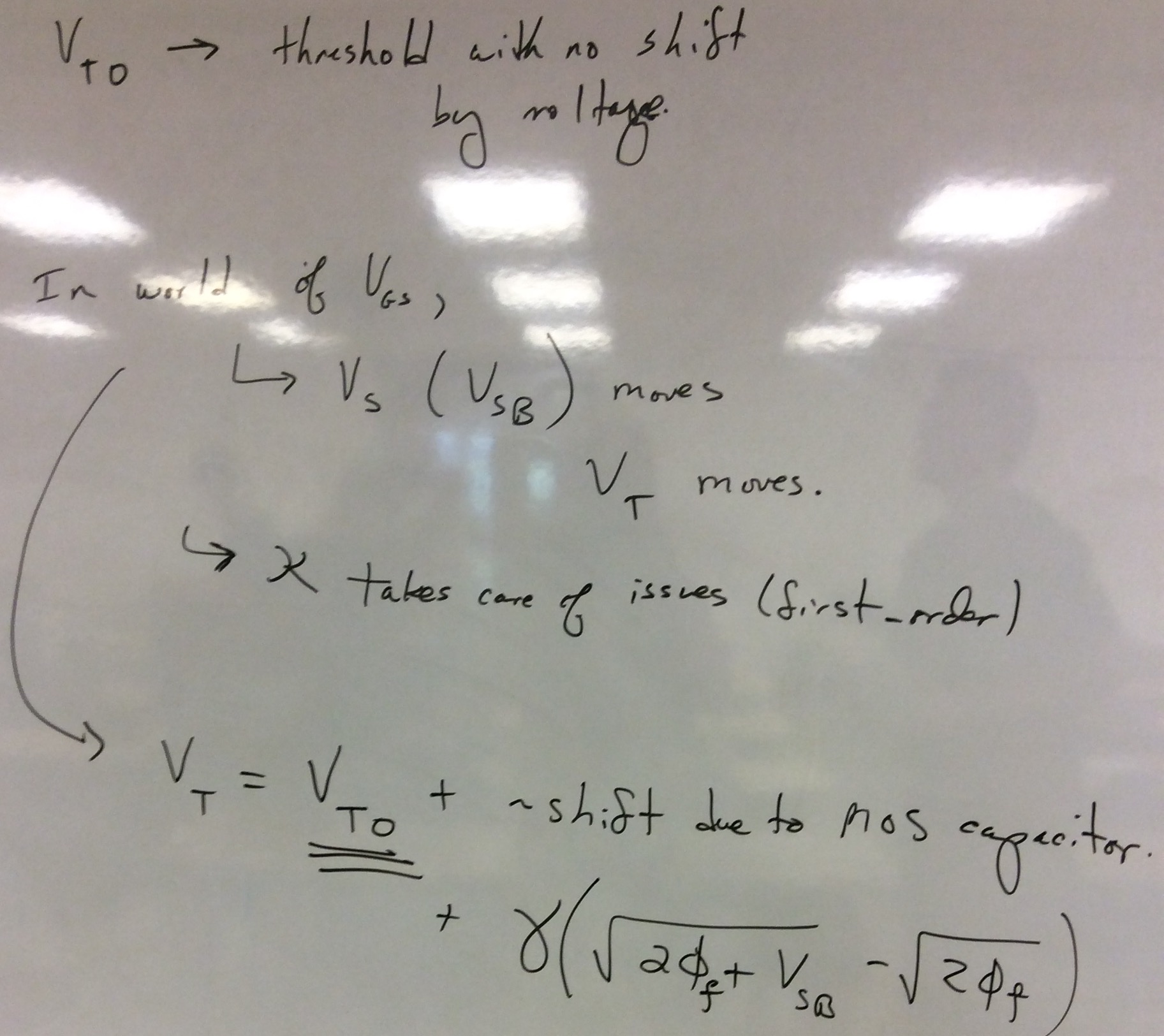
4. Fit the theoretical expression in the above-threshold saturation region of operation (a sqrt() curve fit) for the nFET and pFET curves. Using the results from the above-threshold ohmic region of operation, identify "kappa". Further, extract the value for VT0 and compare with other measurements. Identify any interesting / unexpected parts of the graph.
5. Make a final table of the extracted parameters from these measuremetns.
6. Starting from your extracted parameters, make an nFET and pFET spice model for these gate sweeps where the simulation curves should closely approximate the transistor operation in subthreshold and above threshold currents as well as in the ohmic and saturated sweeps. Your parameters might have to be slightly modified to accomplish this task. "kappa" tends to be represented by "gamma" and "phi" in the spice-level EKV model.
7. You should include saturation and one ohmic figures for this experiment showing Ids versus Vg curve subthreshold operation (exponential current) and above threshold operation. You can make separate plots for the nFET and one for the pFET cases, or you can make one plot for both with voltages relative (as appropriate) to the substrate (the better case for if possible for submission).
In both plots you should show the experimental data,
the appropriate curve fiti(s),
and the resulting simulation curves.
Not plotting these items together means you will not get credit for these efforts.
One expects these overlapping curves, with point markers for the data points (e.g. "o")
and lines for the curve fits and simulation curves.
Please directly label the different data curves on the graph as well as
have useful information also listed on the graph.
The graphs should not have a title, but they should have proper x- and y-axes.
Please refrain from using legends, but rather label the various curves on the graph directly
(gtext(' ') in MATLAB will be very useful).
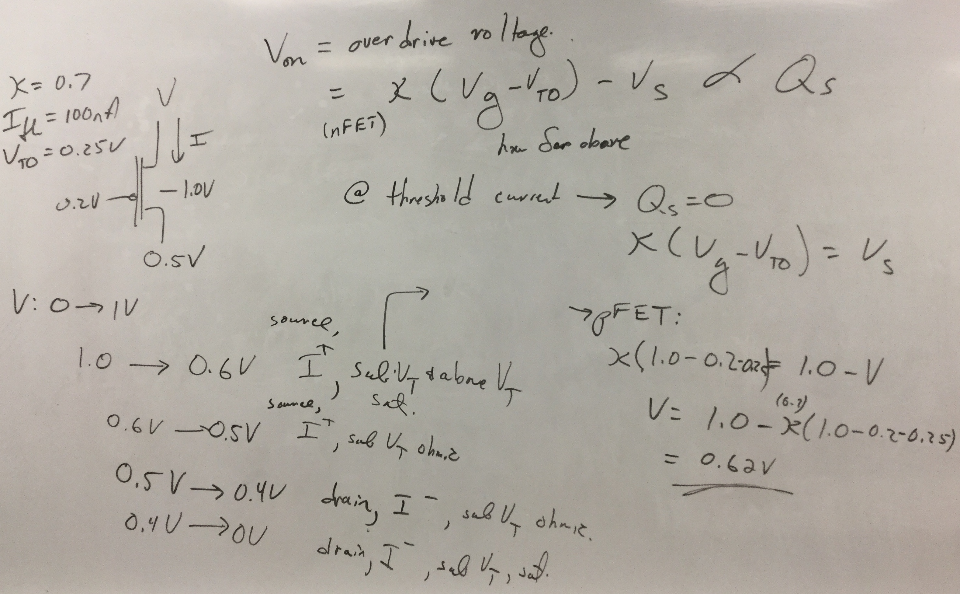
8. In simulation for the nFET and pFET using the models you created that fits the measured data well, perform a source voltage sweep (measuring current) and make a plot of the nFET and pFET data, curve-fitting the subthreshold regime, and address where the curve crosses the threshold current. A measurement of source current versus source voltage swept for a device with the gate and drain voltage held at Vdd / GND (pFET / nFET) for the device operating in saturation throughout the sweep. You should include a figure for this experiment showing Ids versus Vs curve showing subthreshold operation (exponential current). You should get a good subthreshold region as well as part of the above threshold region. Make sure to identify the proper region on the graph. From the subthreshold graph, you should extract a value for UT. Does this value agree with the expected value at room temperature?
Might want the EKV fitting functions (from Bradly A. Minch, Olin U): http://madvlsi.olin.edu/circuits/labs/fits.zip
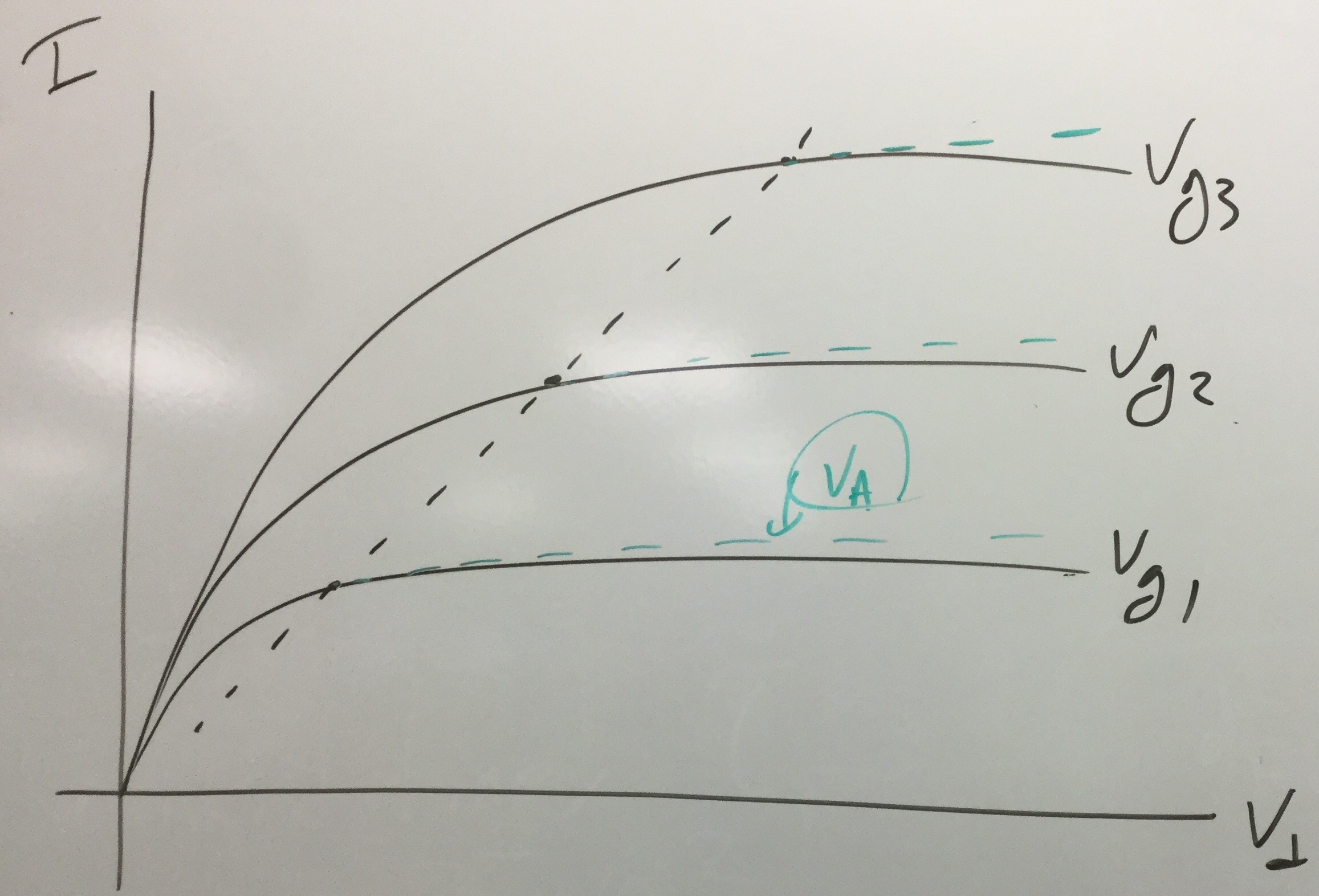
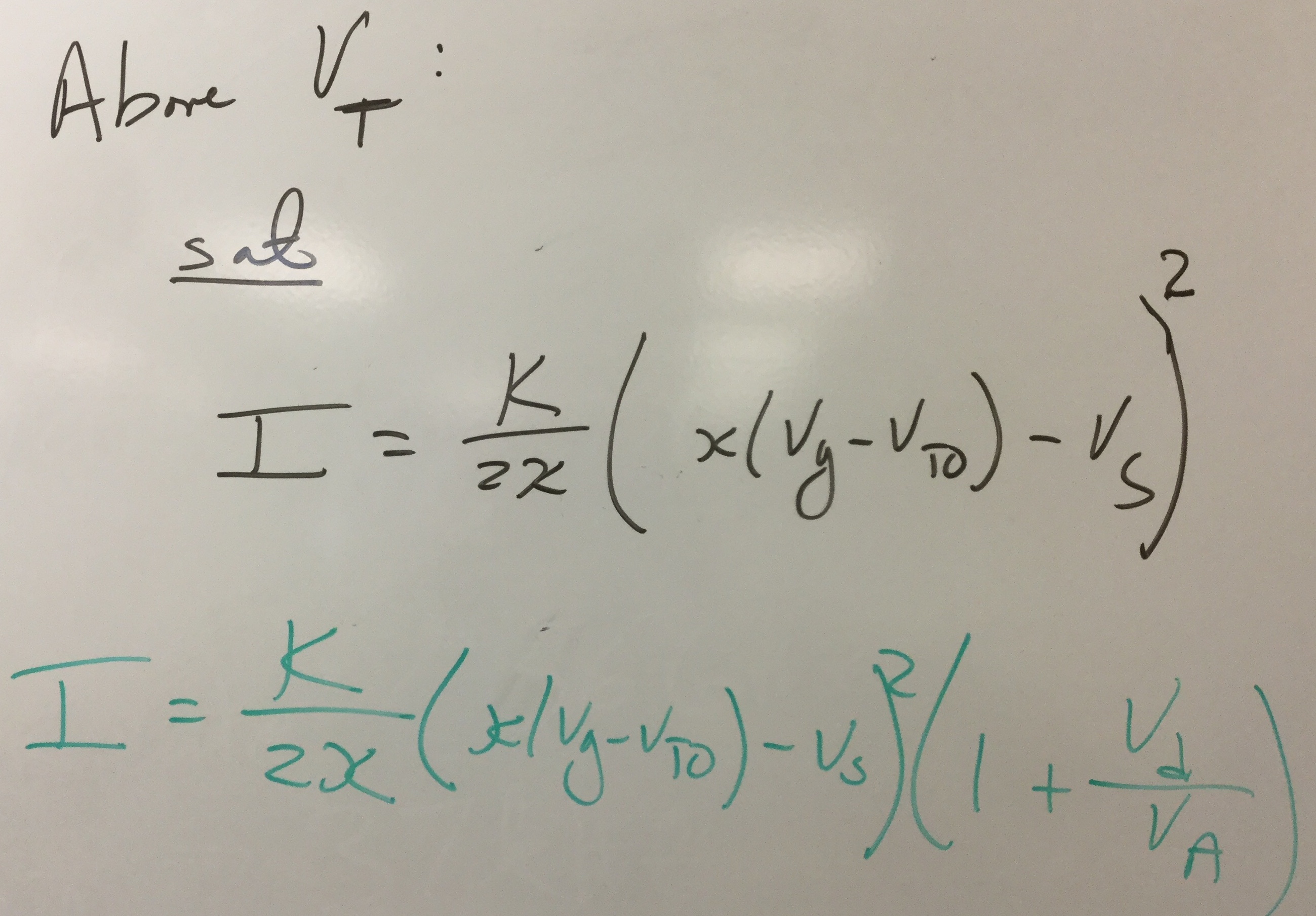
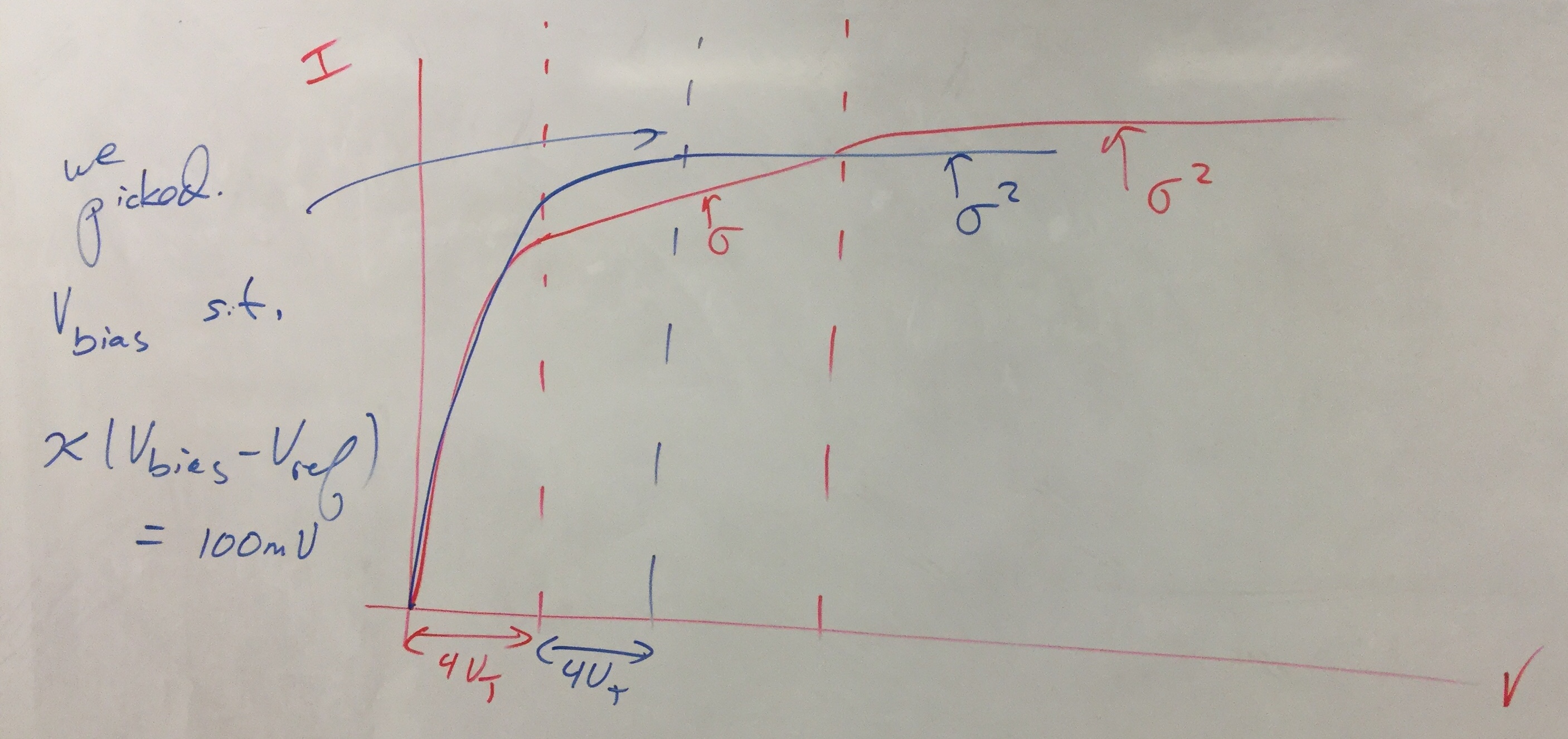
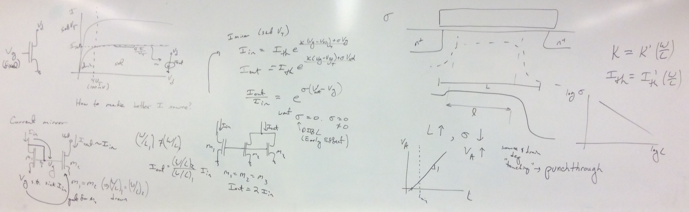
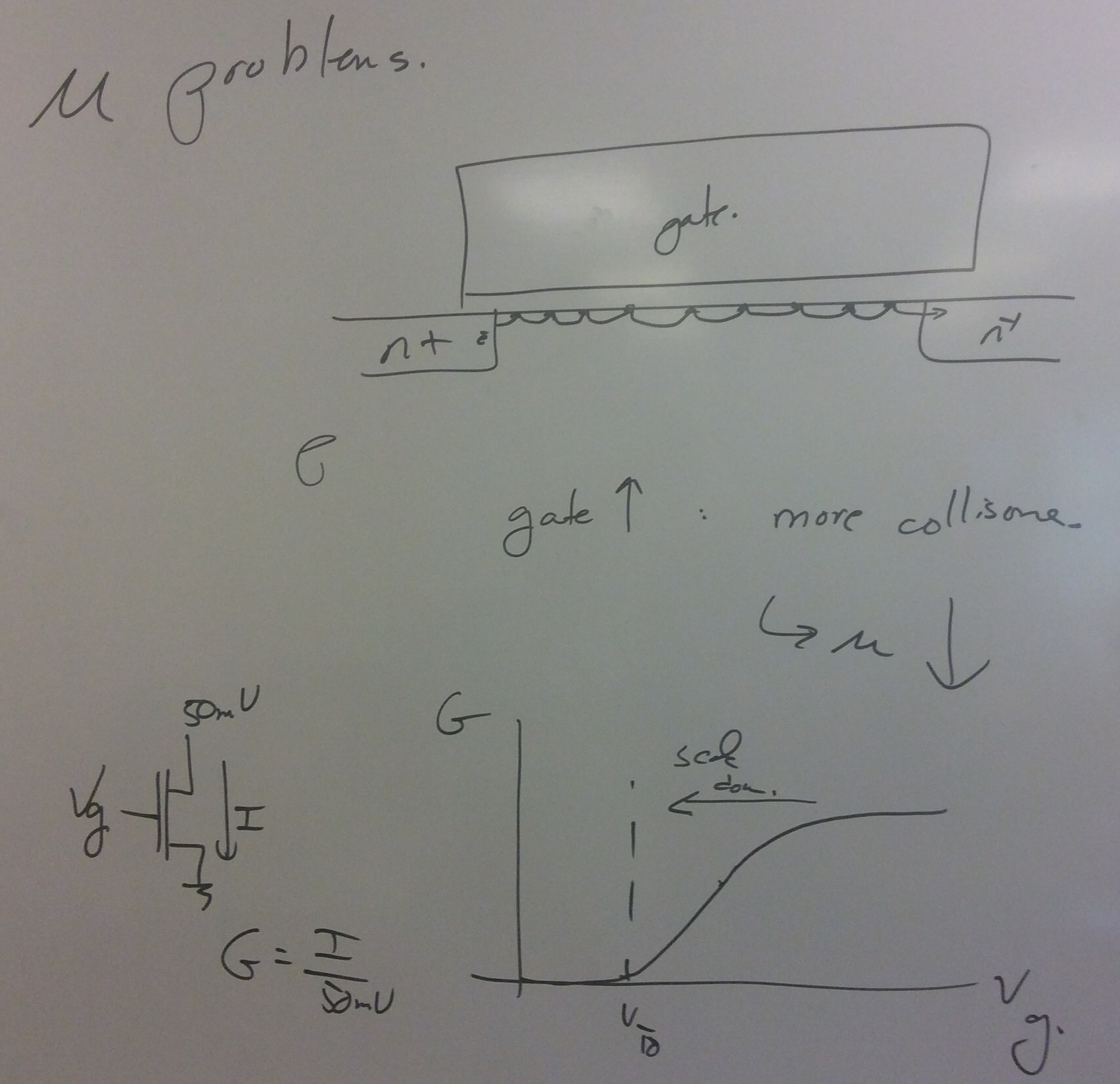
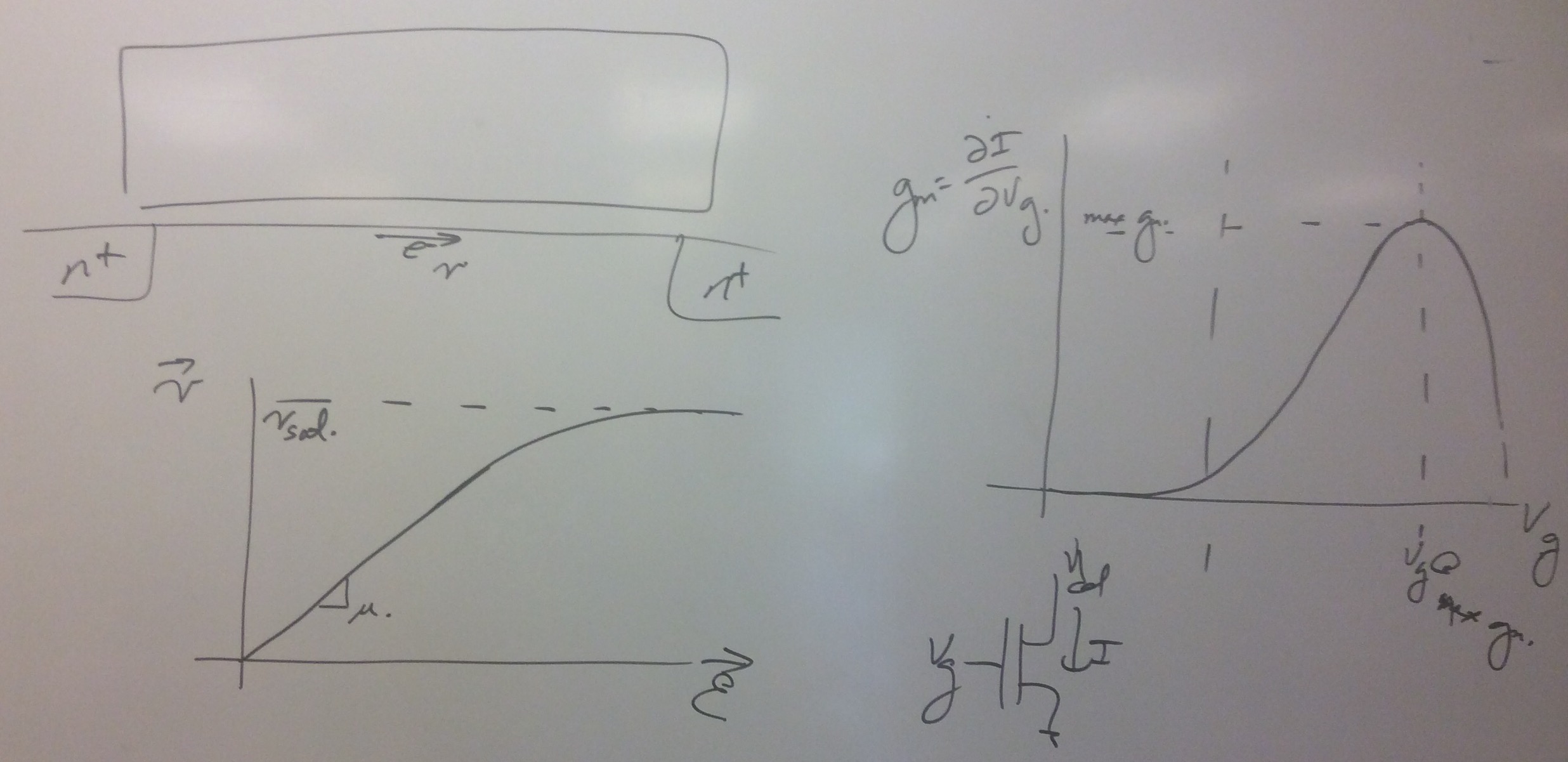
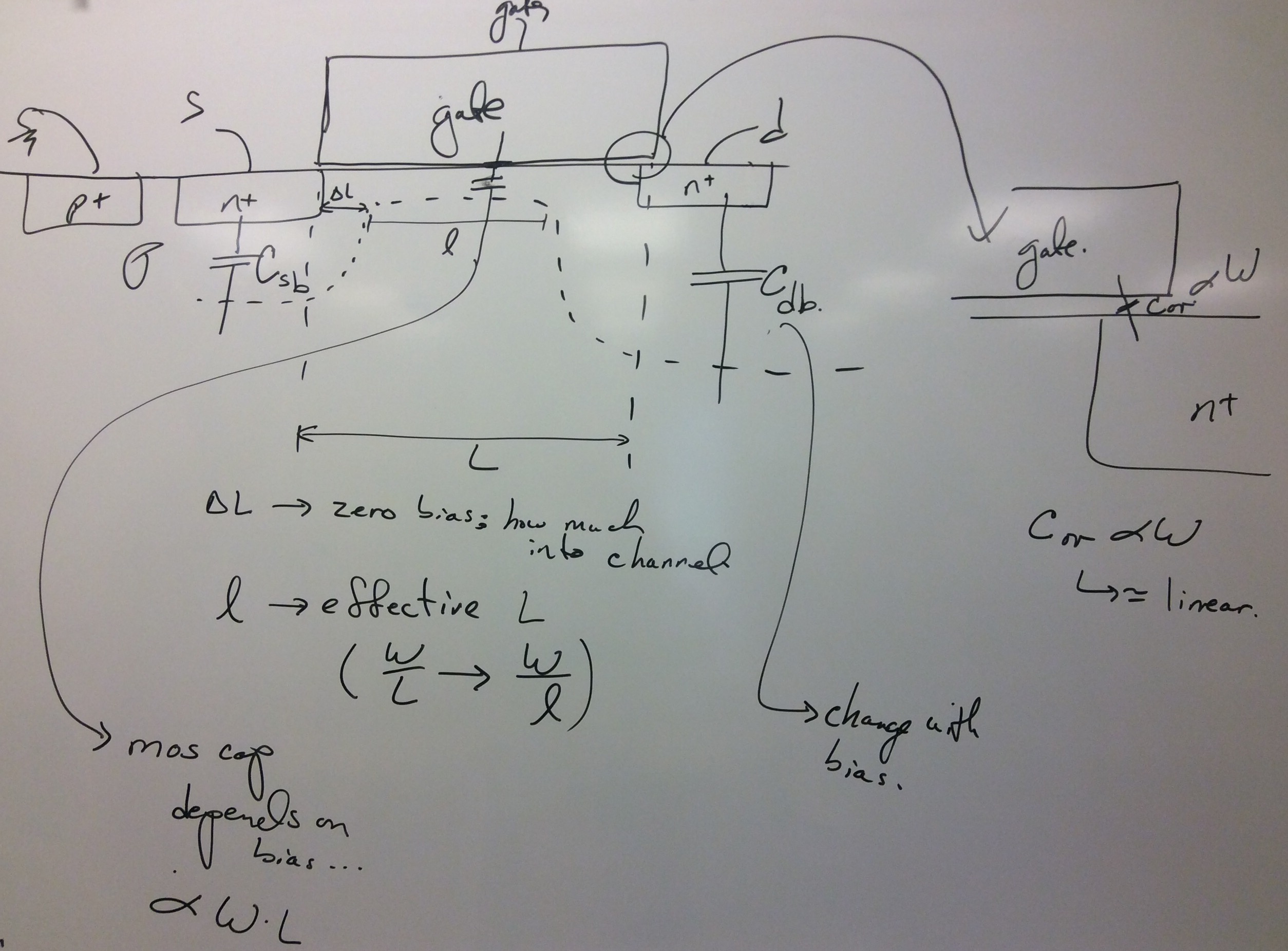
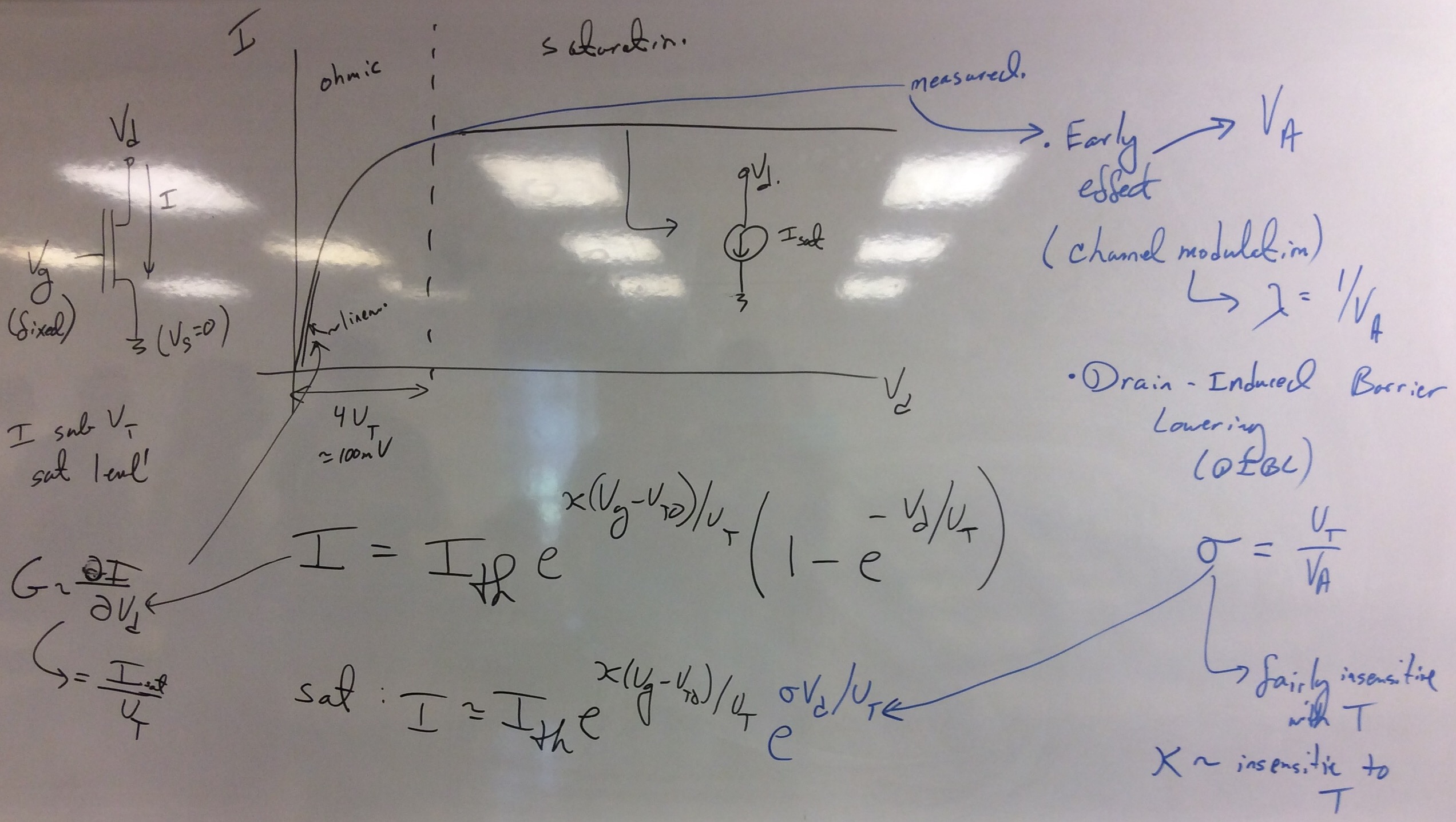
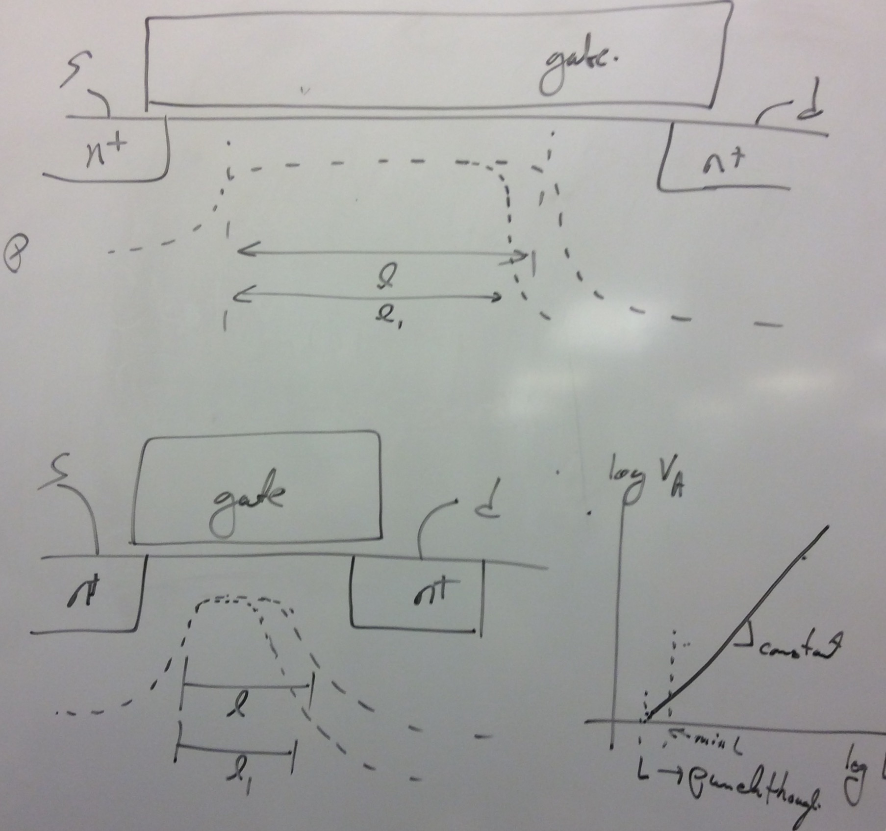
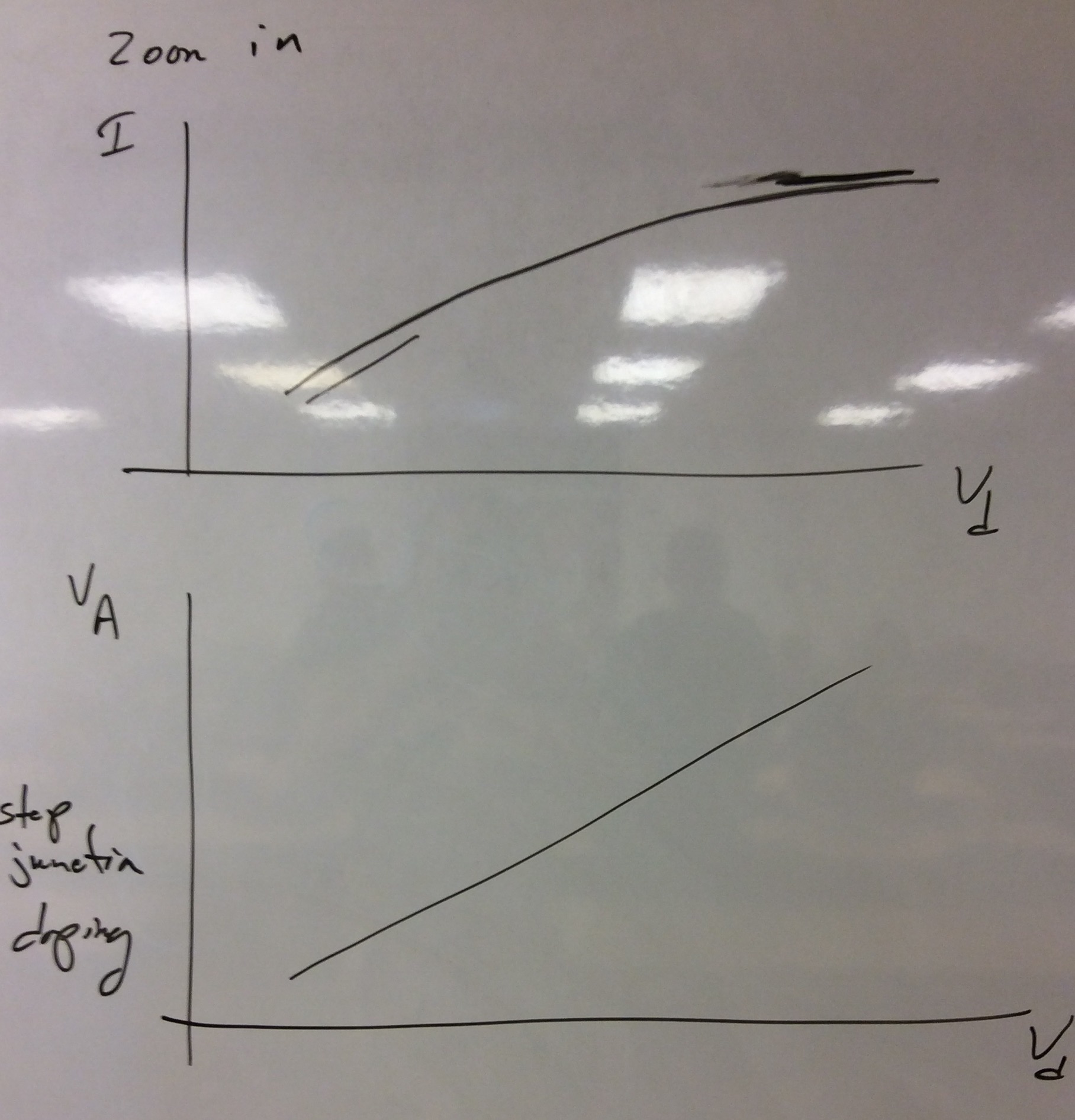
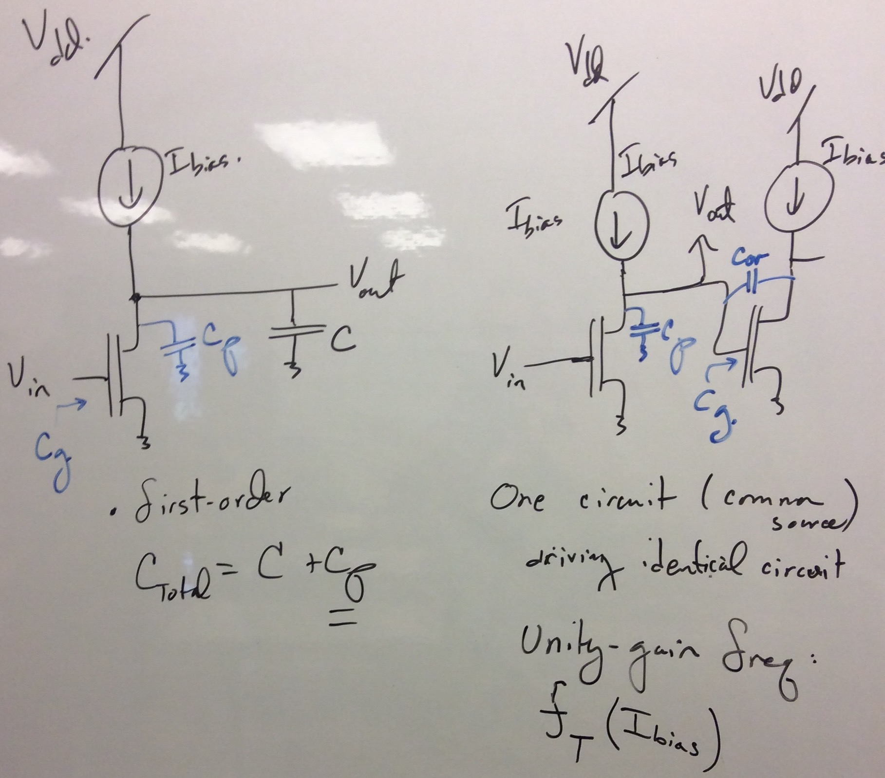
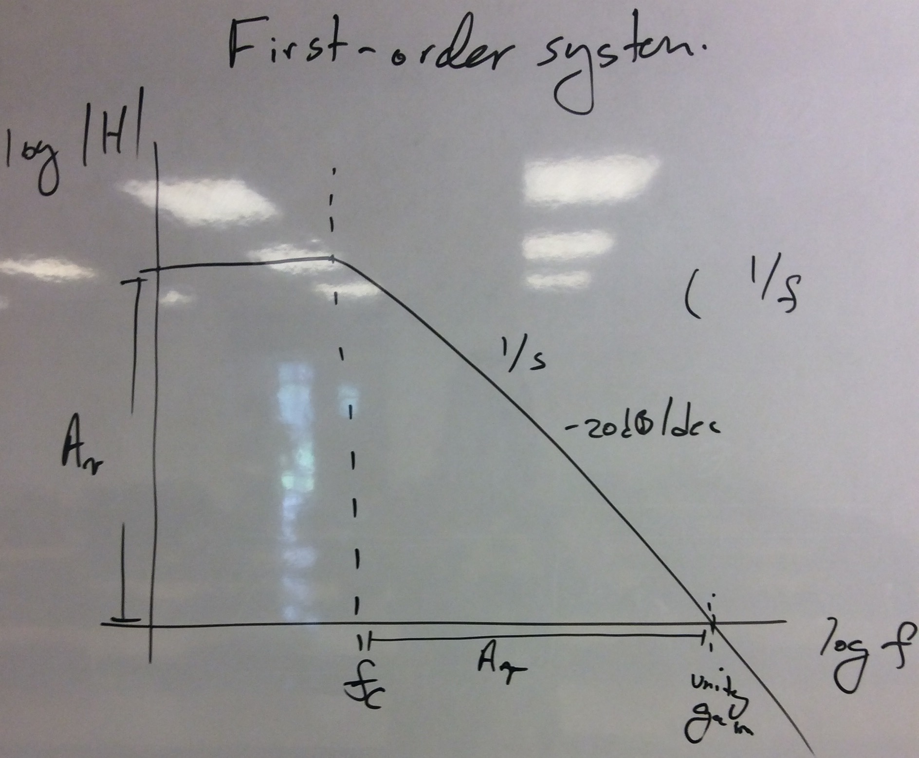
This setion looks at the dependance of the MOSFET Channel Current on Drain Voltage. This dependance illustrates that transistors are a Tunable Current Source. The Early Effect shows that deviation from an ideal current source.
For the given nFET and pFET channel current as a function of drain voltages, ( the source voltage is connected to ground or 0V for the nFET and Vdd for the pFET, and the gate was connected to different fixed voltages for the nFET and pFET)
1. Find the drain-induced barrier lowering ("sigma") / Early voltage (VA) by curve fitting each of the given data sets. Identify the gate voltage for each sweep. It is helpful to select a one volt drain voltage fit range for a saturated current.
2. Perform a simulation that gives similar results using the parameters you previously obtained.
3. Make plots that include the curve fits and simulations on the same plot. You should use point markers (e.g. 'o') for data and straight lines for curve fits and sims. Avoid using a legend, but rather identify the graphs directly with the data where possible. You should show a curve fit in a reasonable region (not over the entire graph).
Identify the ohmic and saturation regimes for the sub- or above-threshold currents. Is this curve taken in subthreshold or above-threshold operation? How could you tell just from your data plot? Identify the drain-to-source voltage was required to reach saturation for each curve. Label these curves with the values of Idsat, "sigma", and VA. Discuss the different VA for the different biases.
4. Make another simulation for two additonal channel lengths for a single gate voltage used above, and make a single plot showing the Early Voltage change, illustrating the classical shift in Early voltage with channel length.
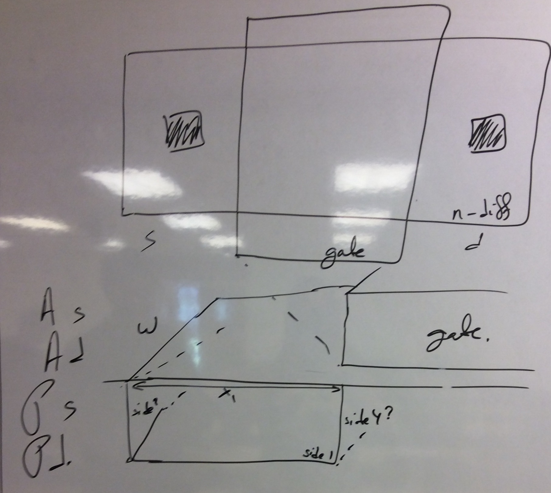
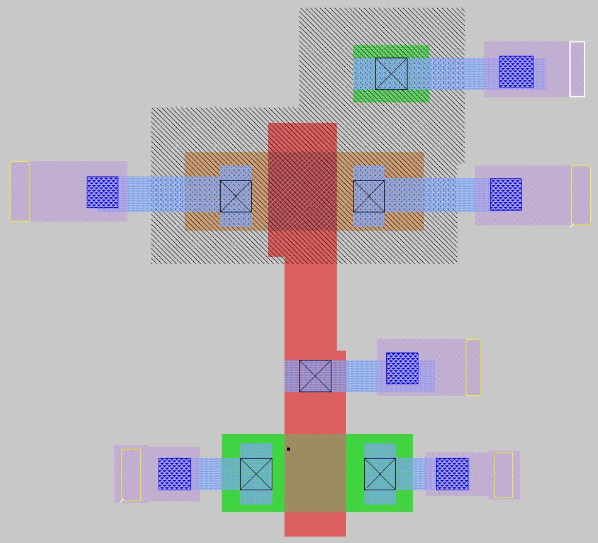
You will need to layout three nFET and three pFET devices.
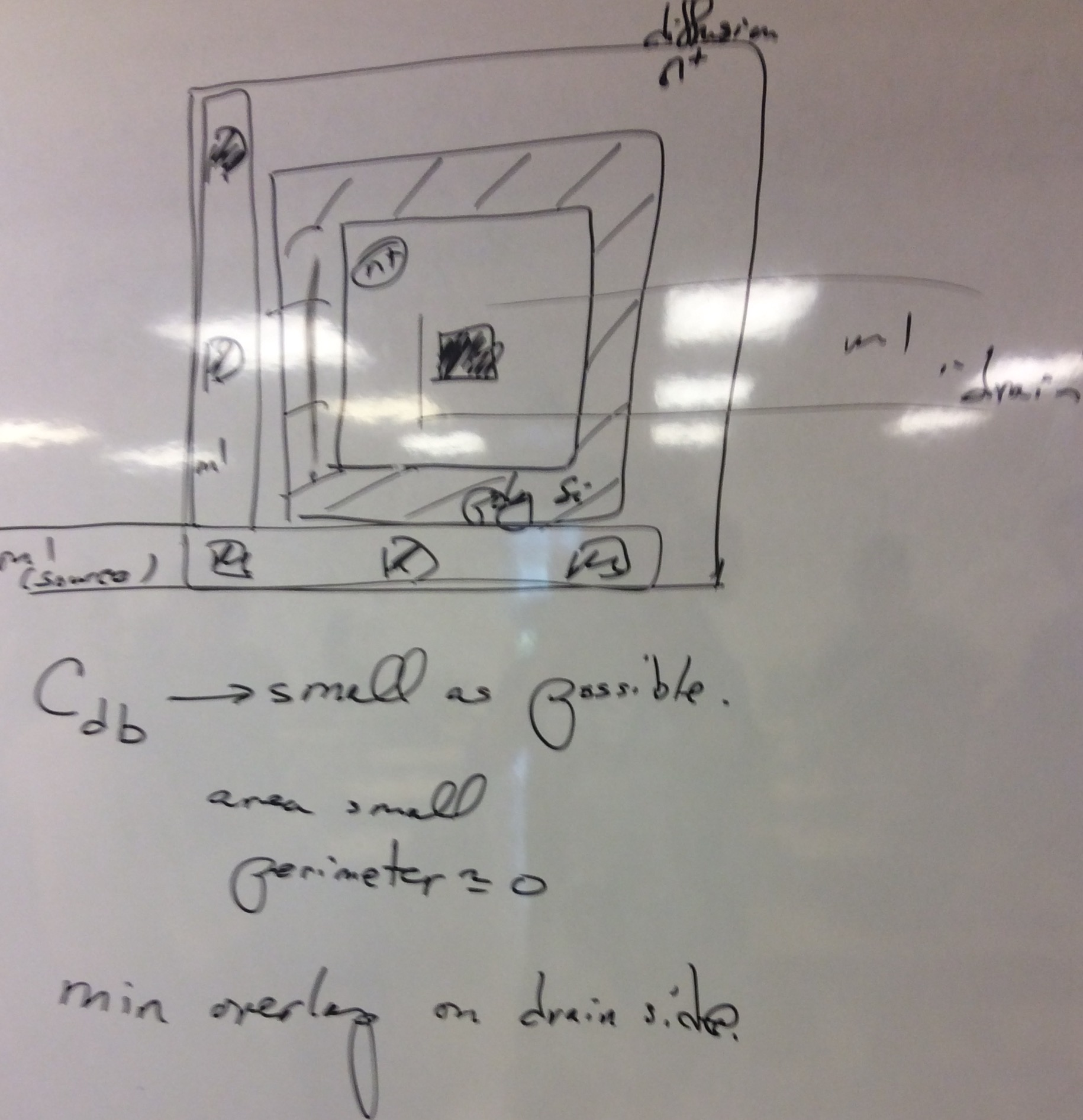
You need to make sure you have extraction of your transistors, showing the resulting parameters (W, L, etc.) that the tools are finding. Verify that the values for area and perimeter that are extracted correspond to the device values that you drew.
You need to perform a gate sweep simulation for each of the devices. Use your extracted model for your simulation.
You should make sure you have substrate or well connections. Terminals should be labeled. This effort will use the Skywater 130nm CMOS technology file.
Previous projects used a Cadence Setup should be set for NCSU technology file, tsmc_02.tf, which roughly corresponds to the 180nm IC process (which sort of worked for 130nm as well). This process is openly available, which is what we will use for this project; in future projects, we might use a more specific process.
magic -T ~/fastlane/pdks/sky130A_hilas/libs.tech/magic/sky130A.tech &
Magic Website location:
http://opencircuitdesign.com/magic/
http://opencircuitdesign.com/magic/magic_docs.html
DRC = Design Rule Check
130nm CMOS process, each grid in Magic is 10nm = 0.01um.
Initial Transistor Example Files: Layout Picture, Magic, Extract, Spice Extraction, Xschem schematic
Short commands:We wanted to include examples from other classes for your reference.
Two video examples for this project are example 1 and example 2 .
Examples from older classes (where a report was required) for 350nm CMOS are
Another set of experimental data for this project: You don't have to do anything with this data, but you might find it helpful. (it is for another CMOS process, so will have very different characteristics).