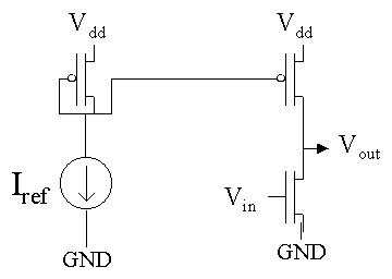
Figure 3: An amplifier with a current source load
| Parameter | nFET | pFET |
| Gate oxide thickness | 40nm | 40nm |
| K' | 1mA/V^2 | 1mA/V^2 |
| Threshold voltage ( VT0 ) | 0.5 | 0.7V |
| "kappa" | 0.68 | 0.74 |
| "Sigma" | 0.001 at 4um | 0.002 at 4um |
|
Calculate the small-signal voltage gain of an NMOS common-source amplifier
with PMOS current-source load of the type shown in Fig. 3.
Do the calculations for values of Iref of 100muA, 10muA, and 1muA.
Assume that the dimensions of each of the transistors are W = 100mum and L = 8mum.
|
Figure 3: An amplifier with a current source load |