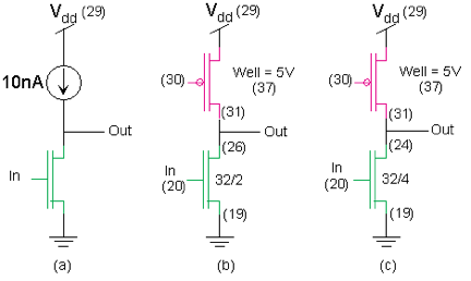
Figure 1: Transistor amplifier circuits
To help your understanding, consider the following questions:

Figure 1: Transistor amplifier circuits
Two transistor Amplifiers : The schematic for the nFET high-gain amplifier is shown in Fig. 1(b,c). Before jumping into the experimental data, first do some initial analysis assuming that these transistors are in subthreshold. "kappa" does not equal 1.

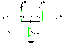
Figure 2: Differential Transistor Pair circuit
Differential Pair Amplifiers : One should go through these questions before attempting the data problems below. You should assume that all MOSFET transistors will be operating in subthreshold throughout this homework set.
Quantitatively show the relationship between transconductance, output resistance, and voltage gain of a transconductance amplifier. Explain how you would measure the voltage gain for a transconductance amplifier if you were given an ammeter and variable voltage source. How will you compute the output resistance, Rout, and transconductance, Gm, from experimental measurements. You will want to show simulation (Scilab/Xcos) results to illustrate your approach.

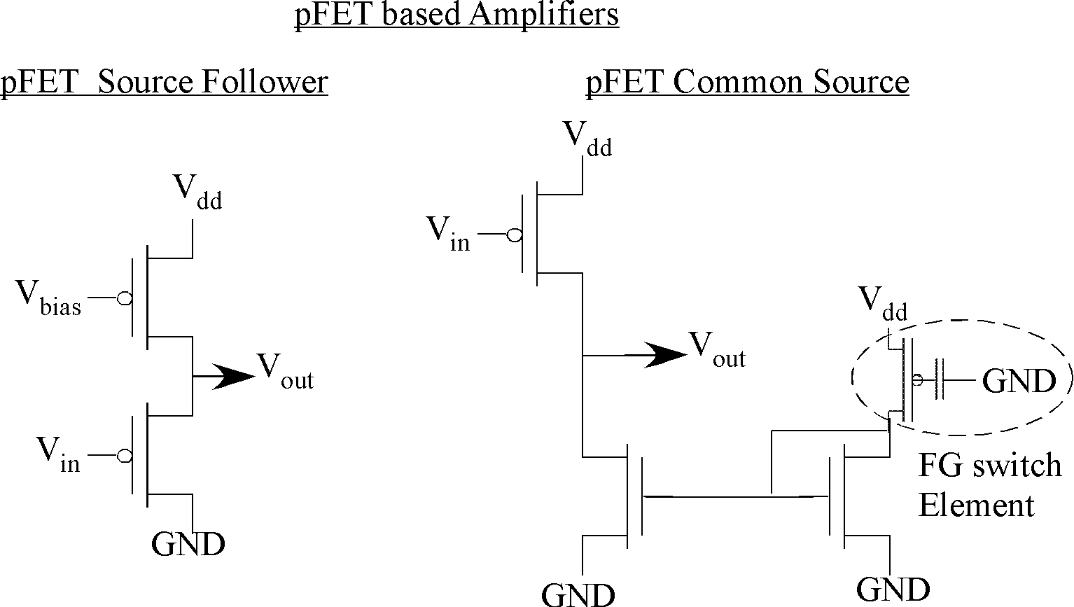
Figure 3: Actual circuit blocks for the pFET source follower and common source experiments. These are the components in the Xcos block elements
Source Follower
Compile a source follower amplifier (pFET active device), and show your resulting high-level file that created your experimental setup. Characterize (make a transfer curve) the follower for at least two bias values. Make a single plot for the transfer function with these bias values. Curve fit these curves to find the gain. Does the response change as a function of the bias values? From your data and analysis of the source follower, you can find kappa as a function of source voltage. It turns out this configuration is a good measurement of how kappa changes for a fixed bias current. Do you notice a change in kappa as a function of source voltage (probably hard to compute a numerical derivative of the data)? Discuss how this change in "kappa" would be related to changes in depletion capacitance.
High Gain Amplifier
Measure the gain of a high-gain transistor amplifier (pFET active device) configured in a common-source configuration. Measure a rough transfer curve (say 25-50mV steps) between the amplifier input and the amplifier output for the two amplifiers. Notice where the data makes a sharp transition, and relate this value to measured parameters and bias voltages. Next perform a dense sweep of the input voltage and measure the resulting output voltage around the high-gain region for the amplifiers ( say at 1mV steps; how to get small steps might require some creativity). This measurement will require some thought given the limited DAC (7bit) resolution.
Make a single plot of these curves, and comment on any noticeable differences, and relate back to the circuits / devices. Curve fit to find the gain in the high-gain region. Compare the amplifier gain to typical values of Early voltage, kappa, and UT; for example, compare to your numbers measured in your previous experiments.
What current level do you estimate this circuit was biased at?
Open loop response (transfer curve) of OTA device : Compile one of the 9-transistor differential amplifiers such that we have the output to an ADC. You will be using a basic transconductance amplifier already built in the CAB, and their should already be a block for that element.
Program a large bias current near the edge of subthreshold operation (i.e. 30nA-100nA). First question is, how do we program and what are we programming? When you pull up your OTA block, there is a parameter asking for the bias current, which is set internally. These parameters program a Floating-Gate (FG) device on-chip, similar to a EEPROM or Flash memory cell, that acts as a current source for the transconductance amplifier. We will cover quite alot more about FG devices throughout the class. What you need to do is do a voltage sweep on the inputs, keeping one input fixed, and measure the output response. Make sure you do not take this data too fast, or the output capacitance will affect your gain measurement. Make a sweep of the output voltage versus input voltage (transfer function). What is the follower gain? Does anything unexpected happen as the input voltage approaches GND? Make a plot (linear scale) of Vout vs. Vin, with a curve fit over the linear (gain) region.
Follower response (Transfer Curve) : We will examine the OTA amplifier connected as a unity-gain device, which we call a follower--integrator circuit (for low frequency operation) Compile and program one of the internal OTAs as a follower circuit with a capacitive load. Since the switches already have capacitance, you might already think your previous circuit compilation should be sufficient, but this time with the - terminal connected to the output. Buffer the output of the IC (therefore only looking at the dynamics from the on-chip behavior). Program the device around 1nA of bias current.
Make a sweep of the output voltage versus input voltage (transfer function). What is the follower gain? Does anything unexpected happen as the input voltage approaches GND? Make a plot (linear scale) of Vout vs. Vin, with a curve fit over the linear region.
Follower-Integrator (time) Response : Apply a small amplitude step input---less than 50mV peak to peak when measured at the input. Make sure that you can see the dynamics of each circuit on the scope. Display both input and output waveforms on a single plot. Repeat for a second bias current level.
Next, Apply a small amplitude step input---greater than 500mV peak to peak when measured at the input. Display both input and output waveforms on a single plot. Repeat at the a second bias current level (or close to that current level).
Determine the time constant of the integrator by curve fitting for your timeconstant (removing steady state, looking at log of the remaining abs of the response). What is the load capacitance? Is there any difference between the rise and fall times? Curve fit response to linear response (exp( -t / tau) ) to determine the time constant of the integrator in both cases, as well as the linear range, where applicable.
Tentitive Project 2 Grading Rubric. The professor reserves the right to change, modify, alter, etc, this document at any time. It is given as a guide of what the rubric might look like.